SLVSAV0B April 2011 – October 2014 TPS55010
PRODUCTION DATA.
- 1 Features
- 2 Applications
- 3 Description
- 4 Simplified Schematic
- 5 Revision History
- 6 Pin Configuration and Functions
- 7 Specifications
-
8 Detailed Description
- 8.1 Overview
- 8.2 Functional Block Diagram
- 8.3
Feature Description
- 8.3.1 Fixed Frequency PWM Control
- 8.3.2 Half Bridge and Bootstrap Voltage
- 8.3.3 Error Amplifier
- 8.3.4 Voltage Reference
- 8.3.5 Adjusting the Output Voltage
- 8.3.6 Enable and Adjusting Undervoltage Lockout
- 8.3.7 Adjusting Slow Start Time
- 8.3.8 Constant Switching Frequency and Timing Resistor (RT/CLK Pin)
- 8.3.9 How to Interface to RT/CLK Pin
- 8.3.10 Overcurrent Protection
- 8.3.11 Reverse Overcurrent Protection
- 8.3.12 FAULT Pin
- 8.3.13 Thermal Shutdown
- 8.4 Device Functional Modes
-
9 Application And Implementation
- 9.1 Application Information
- 9.2
Typical Applications
- 9.2.1 Design Guide - Step-by-Step Design Procedure
- 9.2.2 Primary Side Voltage
- 9.2.3 Voltage Feedback
- 9.2.4 Selecting the Switching Frequency and Primary Inductance
- 9.2.5 Primary Side Capacitor
- 9.2.6 Secondary Side Diode
- 9.2.7 Secondary Side Capacitor
- 9.2.8 Input Capacitor
- 9.2.9 Y - Capacitor
- 9.2.10 Slow Start Capacitor
- 9.2.11 Bootstrap Capacitor Selection
- 9.2.12 UVLO Resistors
- 9.2.13 Compensation
- 9.2.14 Design Tips
- 9.2.15 How to Specify a Fly-Buck Transformer
- 9.2.16 Application Curves
- 9.3 Typical Application, Dual Output
- 10Power Supply Recommendations
- 11Layout
- 12Device and Documentation Support
- 13Mechanical, Packaging, and Orderable Information
Package Options
Mechanical Data (Package|Pins)
- RTE|16
Thermal pad, mechanical data (Package|Pins)
- RTE|16
Orderable Information
9 Application And Implementation
9.1 Application Information
The following design example illustrates how to determine the components for a single output isolated power supply. TI offers an EVM (TPS55010EVM-009) with user guide (SLVU459) and excel calculator tool (SLVC363) to expedite the design process. Additionally the PMP6813 and PMP6838 reference designs show the small solution size possible with the TPS55010. The support material is available on the TPS55010 product folder at www.ti.com.
9.2 Typical Applications
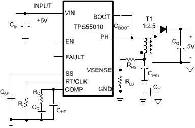 Figure 22. 5 V to 5 V Isolated Power Supply Schematic
Table 1. Reference Design for Common Applications
| 5 V to 5 V at 0.2 A | 3.3 V to 5 V at 0.2 A | 5 V to 3.3 V at 0.3 A | 3.3 V to 3.3 V at 0.3 A | |
|---|---|---|---|---|
| CIN | 47 µF X5R 6.3V | 100 µF X5R 6.3V | 47 µF X5R 6.3V | 100 µF X5R 6.3V |
| COUT | 2 x 10 µF X5R 10V | 47 µF X5R 6.3V | 22 µF X5R 6.3V | 47 µF X5R 6.3V |
| CPRI | 47 µF X5R 10V | 100 µF X5R 6.3V | 100 µF X5R 6.3V | 100 µF X5R 6.3V |
| CBOOT | 0.1 µF X5R 10V | 0.1 µF X5R 10V | 0.1 µF X5R 10V | 0.1 µF X5R 10V |
| CSS | 0.1 µF X5R 10V | 0.1 µF X5R 10V | 0.1 µF X5R 10V | 0.1 µF X5R 10V |
| CCOMP | 5.6 nF | 3.9 nF | 3.3 nF | 3.9 nF |
| CHF | 82 pF | 68 pF | 68 pF | 100 pF |
| RCOMP | 10.5 kΩ | 16.9 kΩ | 18.2 kΩ | 17.4kΩ |
| RHS | 16.5 kΩ | 16.5 kΩ | 8.25 kΩ | 8.25 kΩ |
| RLS | 10.0 kΩ | 10.0 kΩ | 10.0 kΩ | 10.0 kΩ |
| RT | 280 kΩ (350kHz) | 332 kΩ (300kHz) | 402 kΩ (250kHz) | 511 kΩ (200kHz) |
| T1 (See the SLVU459 BOM) | 750311880 | 750311880 | 750311880 | 750311880 |
| D1 | B120 | B120 | B120 | B120 |
9.2.1 Design Guide – Step-by-Step Design Procedure
Table 2. Design Parameters
| PARAMETER | VALUE |
|---|---|
| Input Voltage | 5 V nominal (4.5 V to 5.5 V) |
| Output Voltage | 5 V |
| Output Voltage Ripple | <0.5% |
| Output Current | 200 mA |
| Start Voltage | 4.5V |
| Stop Voltage | 4V |
9.2.2 Primary Side Voltage
The output voltage is a function of the primary voltage, transformer turns ratio and the diode voltage. The primary voltage is a function of the duty cycle and input voltage, and is similar to a step down (buck) regulator as shown in Equation 9. The primary side voltage must be lower than the minimum operating input voltage by 500 mV to avoid maximum duty cycle problems and allow sufficient time for energy transfer during the low side power switch on time. Typically, a primary side voltage that is 50% of the input voltage is ideal to maximize the output power, but 20% to 80% is acceptable. Using the design constraints, the primary side voltage could be from 3.6 V to 1.1 V. A 2.2 V primary side voltage is selected, and the duty cycle is approximately 45%.

9.2.3 Voltage Feedback
9.2.3.1 Turns Ratio
The transformer turns ratio is calculated using the desired output voltage, diode voltage and the primary voltage. Assuming a diode voltage of 0.5 V, VOUT of 5 V, VPRI of 2.2 V yields a NPRI:NSEC turns ratio of 1:2.5.

Selecting 10 kΩ for the RLS, RHS is calculated to be 16.5 kΩ using Equation 11. Choose 100 kΩ as the nearest standard value.
It may be necessary to adjust the feedback resistors to optimize the output voltage over the full load range. Usually checking and setting the output voltage to the nominal voltage at 50% load, yields the best results.

9.2.4 Selecting the Switching Frequency and Primary Inductance
The selection of switching frequency is usually a trade-off between efficiency and component size. However, when isolation is a requirement, switching frequency is not the key variable in determining solution size. Low switching frequency operation improves efficiency by reducing gate drive losses and MOSFET and diode switching losses. However, a lower switching frequency operation requires a larger primary inductance which will have more windings and higher dc resistance.
The optimal primary inductance should be selected between two inductance values, LPRI(MAX) and LPRI(MIN). The primary inductance should be less than LPRI(MAX) for zero voltage switching to improve efficiency and greater than LPRI(MIN) to avoid the peak switch current from exceeding the high side power switch current limit. The recommended minimum and maximum inductance are calculated with Equation 12 and Equation 13. For low output power applications these design equations can suggest too large of an inductance resulting in a small magnetizing current ripple. The ripple current is part of the PWM control system, so the peak-to-peak magnetizing ripple current should be kept above 400 mA for stable and dependable operation. To keep the magnetizing ripple current above 400 mA, make sure the primary inductance value does not exceed the value calculated in Equation 14. Once the primary inductance is selected, check against the low side current limit using the Equation 16 and the high side current limit. For this design example, the switching frequency is selected to be 350 kHz. Using Equation 6, the resistor value is 280 kΩ. LPRI(MAX) and LPRI(MIN) are calculated to be 3.5 µH and 1.2 µH respectively assuming a current limit of 2 A. The maximum inductance using Equation 14 to ensure the magnetizing ripple current is high enough is 8.8 µH. Selecting a primary inductance of the 2.5 µH, the positive and negative peak current are calculated as 1.20 A and -1.99 A in the primary which do not exceed the current limits of the power switch. The rms currents can be calculated and used to determine the power dissipation in the device.
The magnetizing ripple current is calculated as 1.41 A using Equation 17. The highside FET and lowside FET rms currents are calculated as 0.43 A and 0.61 A, respectively using Equation 18 and Equation 19. The sum of these currents, i.e. 1.04 A is the primary side rms current for the magnetics.

Spacer

Spacer

Spacer

Spacer

Spacer

Spacer

Spacer


9.2.5 Primary Side Capacitor
The ΔVPRI voltage should be less than 2% of VPRI. The rated RMS current of CPRI should be greater than Equation 21. For this design example, assuming the ΔVPRI is 0.044 V, the primary side capacitance is 24 µF and the rms current is 1.04 A. A 47 µF/6.3 V X5R ceramic capacitor is used.
Spacer

Spacer

Spacer

Spacer

9.2.6 Secondary Side Diode
The diode should be selected to handle the voltage stress and rms current calculated in Equation 25 and Equation 26. Typically, a low duty cycle or high turns ratio design will have a larger voltage stress on the diode. At the maximum input voltage of 5.5V, the Vdiode_max voltage is calculated at 13.3 V. The rms current is calculated as 0.31 A. The diode peak current is 0.71 A using Equation 27 and the power dissipated in the diode is 0.1 W. The B120 diode is used which is rated for 20 V and 1 A.

Spacer

Spacer

Spacer

9.2.7 Secondary Side Capacitor
The ΔVCO voltage should be 0.25% to 1% of VCO voltage. The converter transfers energy each switching period to the secondary, since the converter has primary side feedback, at light or no load conditions the output voltage may rise above the desired output. If the application will experience a no load condition, attention to the capacitor voltage ratings should be considered. Adding a ballast load, zener diode or linear regulator can help prevent the overvoltage at light or no load.
The output capacitance is calculated to be 10.1 µF using Equation 29 and the rms current is 0.24 A.
Two 10 µF/10V X5R ceramic capactors are used. The effective capacitance is lower than the 20 µF, because of dc voltage bias.

Spacer

9.2.8 Input Capacitor
The ΔVCIN voltage should be 0.25% to 1% of VIN. The TPS55010 requires a high quality ceramic, type X5R or X7R, input decoupling capacitor of at least 2.2 µF of effective capacitance or larger coupled to VIN and GND pins and in some applications additional bulk capacitance. The effective capacitance includes any DC bias effects. The voltage rating of the input capacitor must be greater than the maximum input voltage. In applications with significant unload transients, the bulk input capacitance must be sized to include energy transfer from the primary side capacitor to the input capacitor. The capacitor must also have a ripple current rating greater than the maximum input current ripple of the TPS55010.
The input ripple current can be calculated using Equation 33. The value of a ceramic capacitor varies significantly overtemperature and the amount of DC bias applied to the capacitor. The capacitance variations due to temperature can be minimized by selecting a dielectric material that is stable over temperature. X5R and X7R ceramic dielectrics are usually selected for power regulator capacitors because they have a high capacitance to volume ratio and are fairly stable overtemperature. The output capacitor must also be selected with the DC bias taken into account. The capacitance value of a capacitor decreases as the DC bias across a capacitor increases.
The input capacitor should be larger than the values calculated in Equation 31 and Equation 32. For this design, the calculated minium input capacitance is 12.6 µF using Equation 31 and the rms current is 0.46 A. A 47 µF/10V X5R ceramic capacitor is used on the input. A 0.1 µF ceramic capacitor is placed as close to the VIN and GND pins as possible for a good bias supply.

Spacer

Spacer

9.2.9 Y – Capacitor
The Y-capacitor should be used between the primary and secondary to attenuate common mode (CM) noise in noise sensitive applications. When connecting the primary and secondary grounds with a large loop area, the primary side switching noise can be injected via the interwinding capacitance of the isolation transformer, creating common mode noise in the secondary. A Y-capacitor can be used to provide a local return path for these currents with a small capacitor connected between the secondary ground and the primary ground. The voltage rating of the Y-capacitor should be equivalent to the transformer insulation voltage. If the converter is used for safety isolation there is an upper limit on the amount of capacitance. The inter-winding capacitances of the transformer and maximum leakage current (e.g. UL60950 Class I equipment leakage current <3.5 mA) allowed by the safety standard will set the maximum value. It is not recommended to use the Y-capacitor in applications which experience large voltage transients such as a floating gate drive supply in a power inverter.
9.2.10 Slow Start Capacitor
To minimize overshoot during power up or recovery from an overload condition a slow start capacitor is used. A 35-ms slow start is desired and using Equation 5 a 0.1 µF capacitor is calculated.
9.2.11 Bootstrap Capacitor Selection
A 0.1 µF ceramic capacitor must be connected between the BOOT pin and PH pin for proper operation. It is recommended to use a ceramic capacitor with X5R or better grade dielectric. The capacitor should have 10 V or higher voltage rating.
9.2.12 UVLO Resistors
Using the start and stop voltages of 4.5 V and 4 V, respectively, the UVLO resistors 71.5 kΩ and 26.7 kΩ are calculated using Equation 3 and Equation 4.
9.2.13 Compensation
There are several methods used to compensate DC/DC regulators. The method presented here uses the model of the PWM modulator in the SLVC363 excel tool to choose the compensation components. For most optimized loop compensation, the gain and phase of the PWM modulator can be measured with a network measurement tool.
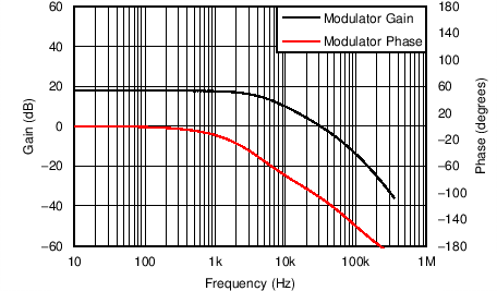
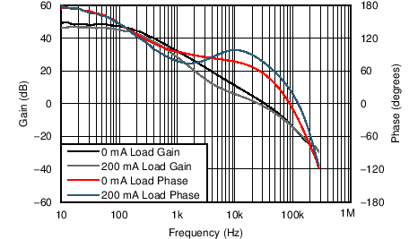
Compensation of a Fly-Buck converter should be done at no load when the loop response is similar to that of a buck converter. With a 47 µF primary capacitor Type 2 compensation is recommended providing a phase boost typically of 165 degrees. For 60 degrees of phase margin, the modulator phase must then be above –105 degrees. The target loop bandwidth is then the frequency when the modulator phase is –105 degrees. Figure 23 shows the modeled modulator frequency response. When modeling the frequency response of the modulator, make sure to include the derating of the ceramic capacitor due to DC bias. In this example the 47 µF capacitor was derated to 36 µF. From this, the target frequency is 29 kHz where the gain is 0.75 dB. With the modulator gain, the value of RC is chosen to set the gain of the compensated error amplifier at the reciprocal of the modulator gain with Equation 34. CC is then chosen to place a zero at 1/10 the target bandwidth with Equation 35. CHF from the COMP pin to ground attenuates high frequency noise. This is selected to add a pole at half the switching frequency with Equation 36. In this example, the final standard values for the compensation are RC = 10.5 kΩ, CC = 5600 pF and CHF = 82 pF.

spacer

spacer

9.2.14 Design Tips
In applications operating near the maximum input voltage (for example 5 V and higher) and at high risk for overload conditions on the output, a bulk ceramic input capacitor with low ESR may be necessary to keep the input voltage stable. If the low-side MOSFET turns off while sinking current nnergy is transferred back to the input and the additional capacitance is used to absorb this energy. During over load conditions the peak current transferred to the input can be as high as the low-side MOSFET sinking current limit.
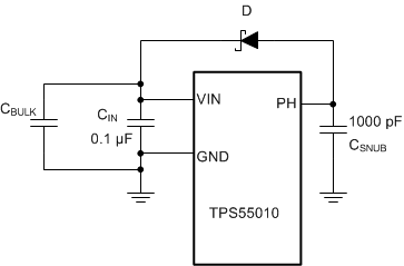
If there is a large ripple on VIN, there is not only risk of exceeding the absolute maximum voltage on the VIN pin, but also on the PH pin. When the low-side MOSFET turns off while sinking current the body diode of the internal high-side MOSFET will conduct for a short dead time period before the high-side MOSFET turns on. While the body diode conducts, the PH pin voltage is equal to VIN + Vbody. Vbody is 0.8 V typical but can be as high as 1.2 V maximum. The 0.1 µF bypass input capacitor should placed as close as is practically possible to the VIN and GND pins to help minimize high frequency voltage overshoot at the PH pin. Additionally a snubber capacitor located as close as possible to the PH pins and the GND pins with a value of 1000 pF limits the slew rate of the PH node to reduce the voltage stress at the PH pin. To further reduce the voltage stress on the internal low-side MOSFET, an external schottky diode with a low voltage drop can be added from the PH pin to the VIN pin. This bypasses the body diode of the internal high-side MOSFET. Figure 24 shows the added components.
9.2.15 How to Specify a Fly-Buck Transformer
There are two catalog transformers available for the TPS55010. See Table 3
Table 3. Transformers
| Part Number | Specifications | Vendor |
|---|---|---|
| 750311880 | 2.5 µH, 1:2.5 Turns Ratio, Basic Insulation, 2500 Vrms | See the SLVU459 BOM |
| 750311780 | 2.0 µH, 1:8:8 Turns Ratio, Basic Insulation, 2000 Vrms | See the SLVU494 BOM |
If a catalog or standard off the shelf transformer is not available, use this section to determine the transformer specifications to supply a vendor. Selecting the magnetizing inductance is similar to the conventional flyback converter operating in continuous conduction mode. One distinction is the voltage across the transformer during the on time is different. The voltage is the difference in the input voltage and voltage across the primary capacitor. For a conventional flyback, only the input voltage is across the primary. Another distinction is the peak current in the primary is the negative current peak.
Table 4. Transformer Design Form
| PARAMETER | DESCRIPTION | ||
|---|---|---|---|
| Input Voltage Range (V) | |||
| Output Voltage (V) | |||
| Output Current (A) | |||
| Operating Mode | Continuous Conduction Mode | ||
| Primary Voltage (V) | Use Equation 9 and Equation 10 | ||
| Duty Cycle Range (%) | Use Equation 9 | ||
| Turns Ratio (NPRI:NSEC) | Use Equation 10 | ||
| Switching Frequency (Hz) | Use Equation 12 to Equation 16 | ||
| Primary Inductance (H) | Use Equation 12 to Equation 16 | ||
| Peak Current Positive (A) | Use Equation 12 to Equation 16 | ||
| Peak Current Negative (A) | Use Equation 12 to Equation 16 | ||
| Insulation Requirements | Functional, Basic, Reinforced | ||
| Regulatory Agencies/Specification | UL, IEC | ||
| Dielectric Withstand Voltage | AC | DC | |
| Working Voltage | AC | DC | |
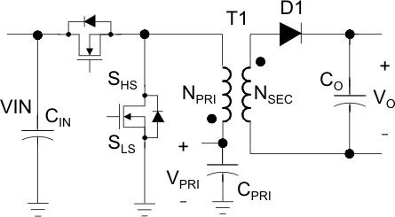 Figure 25. Topology
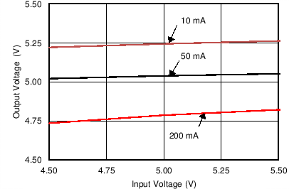
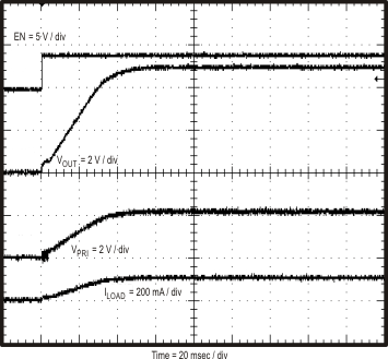
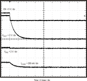
9.2.16 Application Curves
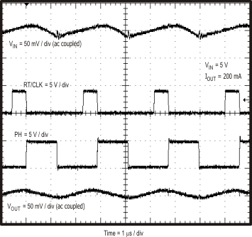
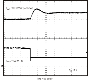
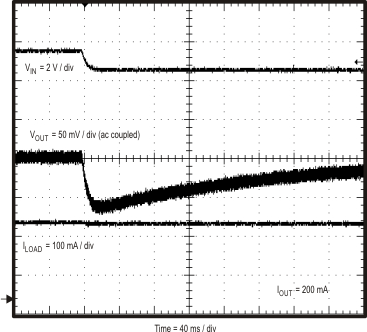
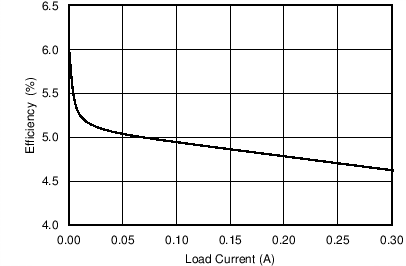
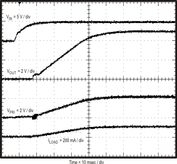
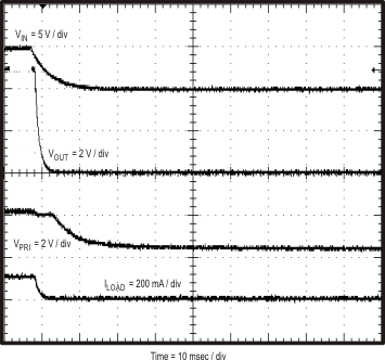
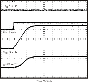
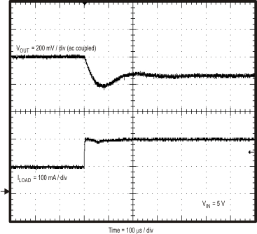
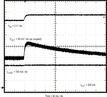
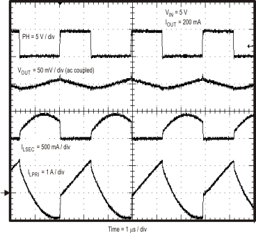
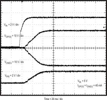
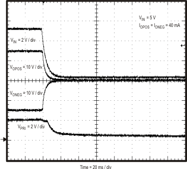
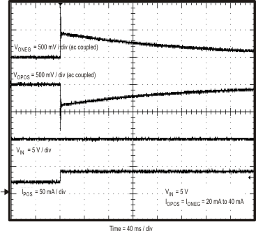
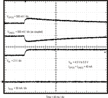
9.3 Typical Application, Dual Output
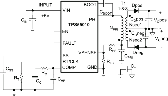 Figure 41. 5 V to 15 V and -15 V Isolated Power Supply
Table 5. Reference Design for Dual Output Application
| 5 V to +15 V and -15 V at 0.04 A each | |
|---|---|
| CIN | 47 µF X5R 6.3V |
| COPOS,CONEG | 10 µF X5R 25V |
| CPRI | 47 µF X5R 10V |
| CBOOT | 0.1 µF X5R 10V |
| CSS | 0.1 µF X5R 10V |
| CC | 3.9 nF |
| CHF | 68 pF |
| RC | 11.0 kΩ |
| RHS | 13.7 kΩ |
| RLS | 10.0 kΩ |
| RT | 243 kΩ |
| T1 | 750311780 (See the SLVU494 BOM) |
| DPOS, DNEG | B1100 |
9.3.1 Design Guide Requirements
Table 6. Design Parameters
| PARAMETER | VALUE |
|---|---|
| Input Voltage | 5 V nominal (4.5 V to 5.5 V) |
| Positive Output Voltage, VO(POS) | +15 V |
| Negative Output Voltage, VO(NEG) | -15 V |
| Output Voltage Ripple | <0.5% |
| Output Current IO(POS), IO(NEG) | 40 mA |
| Start Voltage | 4.5 V |
| Stop Voltage | 4 V |
9.3.2 Detailed Design Procedures
9.3.2.1 Primary Side Voltage for Dual Output
Similar to the single output design, the dual output voltages are a function of the primary voltage, transformer turns ratio and the diode voltages. Using the same design constraints as the single, the primary side voltage could be from 3.6 V to 1.1 V. A 1.93 V primary side voltage is selected, and the duty cycle is approximately 38.5%.

9.3.2.2 Turns Ratio
The transformer turns ratio is calculated using the desired output voltages, diode voltages and the primary voltage. Assuming diode voltages of 0.5 V, VOpos of 15 V, VOneg of -15V and a VPRI of 1.93 V yields a NPRI x NSEC1 x NSEC2 turns ratio of 1:8:8. Since the TPS55010 is flexible on the adjusting the primary side, a couple iterations of selecting turns ratio may help find a solution that is good for multiple applications with the same transformer.

9.3.2.3 Voltage Feedback
Selecting 10 kΩ for the RLS , RHS is calculated to be 13.28 kΩ using Equation 39. Choose 13.7 kΩ as the nearest standard value.

9.3.2.4 Selecting the Switching Frequency and Primary Inductance
For this design example, the switching frequency is selected to be 400 kHz. Using Equation 6, the timing resistor value is 243 kΩ. LOmax and LOmin are calculated to be 2.31 µH and 1.09 µH respectively assuming a current limit of 2 A. Also check that the inductance doesn't exceed the value calculated by Equation 14 to ensure there is enough current ripple for the PWM control system. Selecting a primary inductance of the 2 µH, the positive and negative peak current are calculated as 1.38 A and -2.19 A in the primary which do not exceed the current limits of the power switch. The rms currents can be calculated and used to determine the power dissipation in the device. The magnetizing ripple current is calculated as 1.48 A using Equation 45.
The highside FET and lowside FET rms currents are calculated as 0.478 A and 0.681 A, respectively using Equation 46 and Equation 47. The sum of these currents, i.e. 1.16 A is the primary side rms current for the magnetics.

Spacer

Spacer

Spacer

Spacer

Spacer

Spacer

Spacer

9.3.2.4.1 Primary Side Capacitor
The ΔVPRI voltage should be less than 2% of VPRI. The rated RMS current of CPRI should be greater than Equation 48. For this design example, the charging current and time need to be calculated using Equation 49 and Equation 50. The ICPRI_ch is 0.63 A and the tCPRI is 1.56 µs. Assuming the ΔVPRI is 0.193 V, the primary side capacitance is 25.4 µF using Equation 48. The rms current is 1.16 A from Equation 48. A 47 µF/6.3V X5R ceramic capacitor is used.
Spacer

Spacer

Spacer

Spacer

9.3.2.4.2 Secondary Side Diode
The diodes should be selected to handle the voltage stresses and rms currents calculated in Equation 52 and Equation 54. Typically, a low duty cycle or high turns ratio design will have a larger voltage stress on the diode
At the maximum input voltage of 5.5 V, the Vdiode_max voltage is calculated at 43.56 V. The rms current is calculated as 0.059 A. The diode peak current is 0.130 A using Equation 53 and the power dissipated in the diode is 0.02 W. The B1100 diode will be used which is rated for 100 V and 1 A.
Spacer


Spacer

Spacer

9.3.2.4.3 Secondary Side Capacitor
The ΔVCOPOS and ΔVCONEG voltage should be 0.25% to 1% of the respective nominal voltage. The converter transfers energy each switching period to the secondary, since the converter has primary side feedback, at light or no load conditions the output voltage may rise above the desired output. If the application will experience a no load condition, attention to the capacitor voltage ratings should be considered. Adding a ballast load, zener diode or linear regulator can help prevent the overvoltage at light or no load.
The output capacitance is calculated to be 0.51 µF assuming a ΔVCOPOS of 75 mV using Equation 56 and the rms current is 0.043 A from Equation 57. 10 µF/25 V capacitors are used for VOPOS and VONEG output.

Spacer

9.3.2.4.4 Input Capacitor
The ΔVCIN voltage should be 0.25% to 1% of VIN. The TPS55010 requires a high quality ceramic, type X5R or X7R, input decoupling capacitor of at least 2.2 µF of effective capacitance or larger coupled to VIN and GND pins and in some applications additional bulk capacitance. The effective capacitance includes any DC bias effects. The voltage rating of the input capacitor must be greater than the maximum input voltage. The input ripple current can be calculated using Equation 59, select a capacitor with a larger ripple current rating.
In applications with significant unload transients, the bulk input capacitance must be sized to include energy transfer from the primary side capacitor to the input capacitor. The input capacitor should be larger than the values calculated in Equation 58 and Equation 32. For this design, the input capacitance is calculated 12.4 µF using Equation 58 and the rms current is 0.495 A. A 47 µF/10 V X5R ceramic capacitor is used on the input. A 0.1 µF ceramic capacitor is placed as close to the VIN and GND pins as possible for a good bias supply.
Spacer

Spacer

9.3.2.5 Compensation
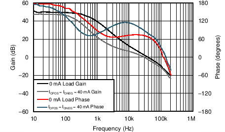
Compensation of the dual output design is the same as the single output presented in Compensation. Using the Model of the PWM modulator in the SLVC363 excel tool the target frequency is 34 kHz and the modulator gain at this frequency is -1.04 dB. Using Equation 34 to Equation 36 the final nearest standard values for the compensation are RC = 11 kΩ, CC = 3900 pF and CHF = 68 pF.
9.3.2.6 Application Curves
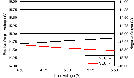
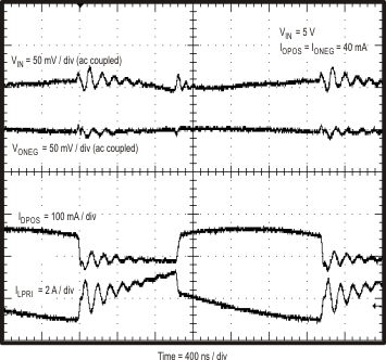
| LOPOS = LONEG = 20 mA |
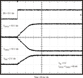
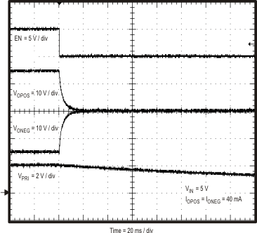
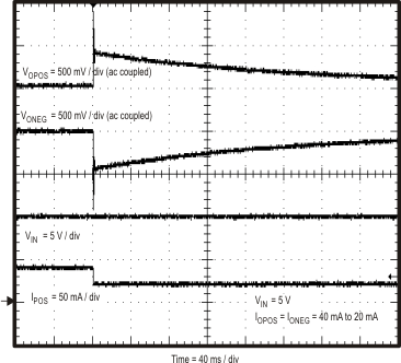
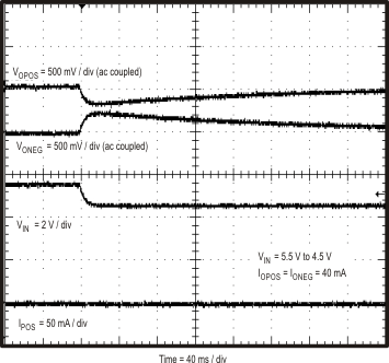
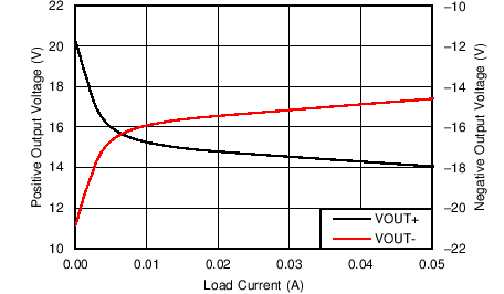
| VIN = 5 V | LOPOS = LONEG |
