SLVSF01B November 2018 – December 2020 TPS55288
PRODUCTION DATA
- 1 Features
- 2 Applications
- 3 Description
- 4 Revision History
- 5 Pin Configuration and Functions
- 6 Specifications
-
7 Detailed Description
- 7.1 Overview
- 7.2 Functional Block Diagram
- 7.3
Feature Description
- 7.3.1 VCC Power Supply
- 7.3.2 Operation Mode Setting
- 7.3.3 Input Undervoltage Lockout
- 7.3.4 Enable and Programmable UVLO
- 7.3.5 Soft Start
- 7.3.6 Shutdown and Load Discharge
- 7.3.7 Switching Frequency
- 7.3.8 Switching Frequency Dithering
- 7.3.9 Inductor Current Limit
- 7.3.10 Internal Charge Path
- 7.3.11 Output Voltage Setting
- 7.3.12 Output Current Monitoring and Cable Voltage Droop Compensation
- 7.3.13 Integrated Gate Drivers
- 7.3.14 Output Current Limit
- 7.3.15 Overvoltage Protection
- 7.3.16 Output Short Circuit Protection
- 7.3.17 Thermal Shutdown
- 7.4 Device Functional Modes
- 7.5 I2C Serial Interface
- 7.6
Register Maps
- 7.6.1 REF Register (Address = 0h, 1h) [reset = 11010010h, 00000000h]
- 7.6.2 IOUT_LIMIT Register (Address = 2h) [reset = 11100100h]
- 7.6.3 VOUT_SR Register (Address = 3h) [reset = 00000001h]
- 7.6.4 VOUT_FS Register (Address = 4h) [reset = 00000011h]
- 7.6.5 CDC Register (Address = 5h) [reset = 11100000h]
- 7.6.6 MODE Register (Address = 6h) [reset = 00100000h]
- 7.6.7 STATUS Register (Address = 7h) [reset = 00000011h]
- 7.6.8 Register Summary
- 8 Application and Implementation
- 9 Power Supply Recommendations
- 10Layout
- 11Device and Documentation Support
- 12Mechanical, Packaging, and Orderable Information
Package Options
Mechanical Data (Package|Pins)
- RPM|26
Thermal pad, mechanical data (Package|Pins)
- RPM|26
Orderable Information
3 Description
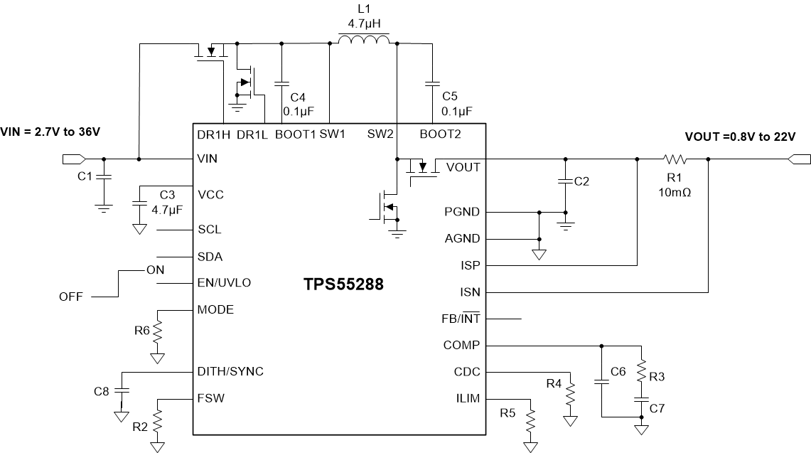
The TPS55288 is a synchronous four-switch buck-boost converter capable of regulating the output voltage at, above, or below the input voltage. The TPS55288 operates over 2.7-V to 36-V wide input voltage and capable of outputing 0.8-V to 22-V voltage to support a variety of applications.
The TPS55288 integrates two 16-A MOSFETs of the boost leg to balance the solution size and efficiency. With the programmable output voltage and output current limit through I2C interface, the TPS55288 is fully compliant to the USB PD specification. The TPS55288 is capable of delivering 100 W from 12-V input voltage.
The TPS55288 employs average current-mode control scheme. The switching frequency is programmable from 200 kHz to 2.2 MHz by an external resistor and can be synchronized to an external clock. The TPS55288 also provides optional spread spectrum to minimize peak EMI.
The TPS55288 offers output over-voltage protection, average inductor current limit, cycle-by-cycle peak current limit and output short circuit protection. The TPS55288 also ensures safe operating with optional output current limit and hiccup-mode protection in sustained overload conditions.
The TPS55288 can use a small inductor and small capacitors with high switching frequency. It is available in 4.0-mm × 3.5-mm QFN package.
| PART NUMBER | PACKAGE(1) | BODY SIZE |
|---|---|---|
| TPS55288 | VQFN-HR | 4.00 mm × 3.50 mm |
 Typical
Application Circuit