SLVSFC5 November 2020 TPS552882
PRODUCTION DATA
- 1 Features
- 2 Applications
- 3 Description
- 4 Revision History
- 5 Pin Configuration and Functions
- 6 Specifications
-
7 Detailed Description
- 7.1 Overview
- 7.2 Functional Block Diagram
- 7.3
Feature Description
- 7.3.1 VCC Power Supply
- 7.3.2 Operation Mode Setting
- 7.3.3 Input Undervoltage Lockout
- 7.3.4 Enable and Programmable UVLO
- 7.3.5 Soft Start
- 7.3.6 Shutdown
- 7.3.7 Switching Frequency
- 7.3.8 Switching Frequency Dithering
- 7.3.9 Inductor Current Limit
- 7.3.10 Internal Charge Path
- 7.3.11 Output Voltage Setting
- 7.3.12 Output Current Indication and Cable Voltage Drop Compensation
- 7.3.13 Integrated Gate Drivers
- 7.3.14 Output Current Limit
- 7.3.15 Overvoltage Protection
- 7.3.16 Output Short Circuit Protection
- 7.3.17 Thermal Shutdown
- 7.4 Device Functional Modes
- 8 Application and Implementation
- 9 Power Supply Recommendations
- 10Layout
- 11Device and Documentation Support
Package Options
Mechanical Data (Package|Pins)
- RPM|26
Thermal pad, mechanical data (Package|Pins)
- RPM|26
Orderable Information
3 Description
The TPS552882 is a synchronous four-switch buck-boost converter capable of regulating the output voltage at, above, or below the input voltage. The TPS552882 operates over a 2.7-V to 36-V wide input voltage and is capable of outputing 0.8-V to 22-V voltage to support a variety of applications.
The TPS552882 integrates two 16-A MOSFETs of the boost leg to balance the solution size and efficiency. The TPS552882 uses an external resistor divider to set the output voltage with 1.2V internal reference voltage. The TPS552882 is capable of delivering 100 W from 12-V input voltage.
The TPS552882 employs average current-mode control scheme. The switching frequency is programmable from 200 kHz to 2.2 MHz by an external resistor and can be synchronized to an external clock. The TPS552882 also provides optional spread spectrum to minimize peak EMI.
The TPS552882 offers output over-voltage protection, average inductor current limit, cycle-by-cycle peak current limit and output short circuit protection. The TPS552882 also ensures safe operating with optional output current limit and hiccup-mode protection in sustained overload conditions.
The TPS552882 can use a small inductor and small capacitors with high switching frequency. It is available in a 4.0-mm × 3.5-mm HotRod QFN package.
| PART NUMBER | PACKAGE(1) | BODY SIZE |
|---|---|---|
| TPS552882 | VQFN-HR | 4.00 mm × 3.50 mm |
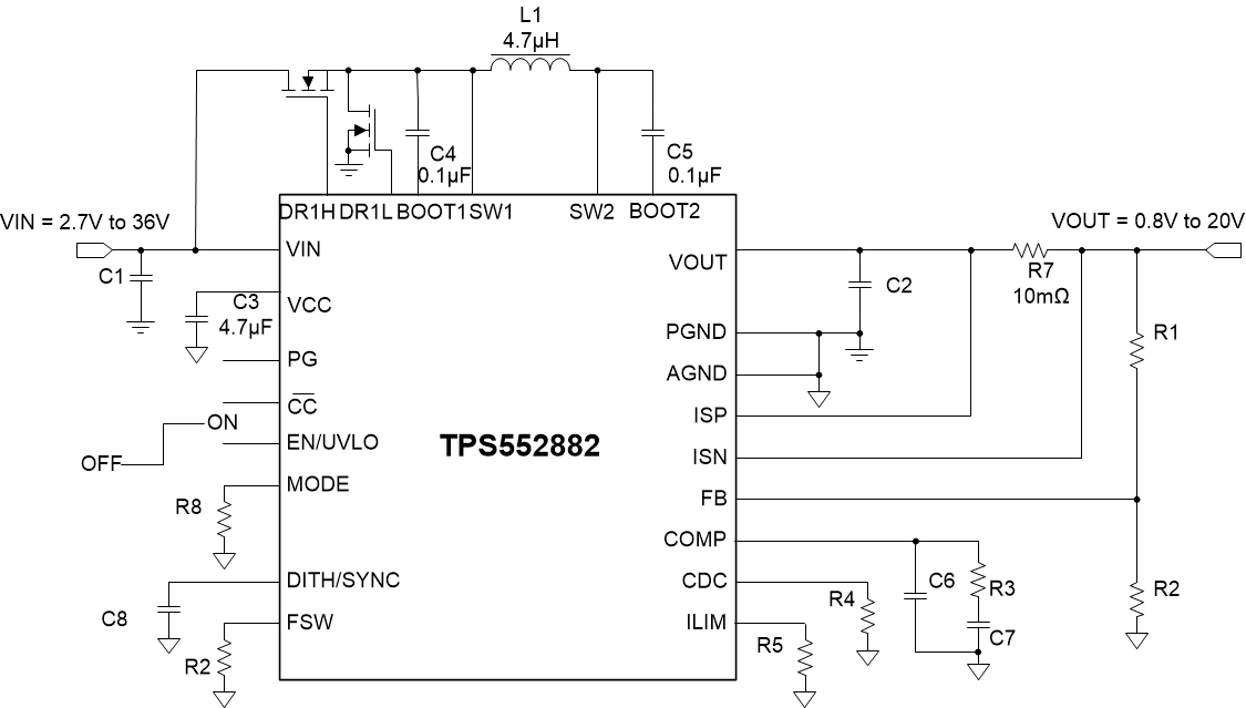
 Typical Application Circuit