SLVSGT7 april 2023 TPS552892-Q1
PRODUCTION DATA
- 1 Features
- 2 Applications
- 3 Description
- 4 Revision History
- 5 Pin Configuration and Functions
- 6 Specifications
-
7 Detailed Description
- 7.1 Overview
- 7.2 Functional Block Diagram
- 7.3
Feature Description
- 7.3.1 VCC Power Supply
- 7.3.2 EXTVCC Power Supply
- 7.3.3 Input Undervoltage Lockout
- 7.3.4 Enable and Programmable UVLO
- 7.3.5 Soft Start
- 7.3.6 Shutdown
- 7.3.7 Switching Frequency
- 7.3.8 Switching Frequency Dithering
- 7.3.9 Inductor Current Limit
- 7.3.10 Internal Charge Path
- 7.3.11 Output Voltage Setting
- 7.3.12 Output Current Monitoring and Cable Voltage Droop Compensation
- 7.3.13 Output Current Limit
- 7.3.14 Overvoltage Protection
- 7.3.15 Output Short Circuit Protection
- 7.3.16 Power Good
- 7.3.17 Constant Current Output Indication
- 7.3.18 Thermal Shutdown
- 7.4 Device Functional Modes
- 8 Application and Implementation
- 9 Device and Documentation Support
- 10Mechanical, Packaging, and Orderable Information
Package Options
Mechanical Data (Package|Pins)
- RYQ|21
Thermal pad, mechanical data (Package|Pins)
- RYQ|21
Orderable Information
7.3.8 Switching Frequency Dithering
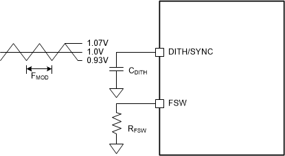
The TPS552892-Q1 provides an optional switching frequency dithering that is enabled by connecting a capacitor from the DITH/SYNC pin to ground. Figure 7-4 illustrates the dithering circuit. By charging and discharging the capacitor, a triangular waveform centered at 1 V is generated at the DITH/SYNC pin. The triangular waveform modulates the oscillator frequency by ±7% of the nominal frequency set by the resistance at the FSW pin. The capacitance at the DITH/SYNC pin sets the modulation frequency. A small capacitance modulates the oscillator frequency at a fast rate than a large capacitance. For the dithering circuit to effectively reduce peak EMI, the modulation rate normally is below 1 kHz. Equation 4 calculates the capacitance required to set the modulation frequency, FMOD.

where
- RFSW is the switching frequency setting resistance (Ω) at the FSW pin
- FMOD is the modulation frequency (Hz) of the dithering
Connecting the DITH/SYNC pin below 0.4 V or above 1.2 V disables switching frequency dithering. The dithering function also is disabled when an external synchronous clock is used.
 Figure 7-4 Switching Frequency Dithering