SLVS939B June 2009 – December 2014 TPS55332-Q1
PRODUCTION DATA.
- 1 Features
- 2 Applications
- 3 Description
- 4 Revision History
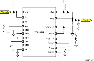
- 5 Pin Configuration and Functions
- 6 Specifications
-
7 Detailed Description
- 7.1 Overview
- 7.2 Functional Block Diagram
- 7.3
Feature Description
- 7.3.1 Input Voltage (VIN)
- 7.3.2 Output Voltage (Vout)
- 7.3.3 Regulated Supply Voltage (VReg)
- 7.3.4 Over-Current Protection (SW)
- 7.3.5 Oscillator Frequency (RT)
- 7.3.6 Enable / Shutdown (EN)
- 7.3.7 Reset Delay (Cdly)
- 7.3.8 Reset Pin (RST)
- 7.3.9 Boost Capacitor (BOOT)
- 7.3.10 Soft Start (SS)
- 7.3.11 Synchronization (SYNC)
- 7.3.12 Regulation Voltage (VSENSE)
- 7.3.13 Reset Threshold (RST_TH)
- 7.3.14 Slew Rate Control (Rslew)
- 7.3.15 Thermal Shutdown
- 7.3.16 Loop Control Frequency Compensation
- 7.4 Device Functional Modes
-
8 Application and Implementation
- 8.1 Application Information
- 8.2
Typical Application
- 8.2.1 Design Requirements
- 8.2.2
Detailed Design Procedure
- 8.2.2.1 Output Capacitor (Co)
- 8.2.2.2 Output Inductor Selection (Lo) for CCM
- 8.2.2.3 Output Diode
- 8.2.2.4 Input Capacitor CI
- 8.2.2.5 Output Voltage And Feedback Resistor Selection
- 8.2.2.6 Reset Threshold Resistor Selection
- 8.2.2.7 Soft Start Capacitor
- 8.2.2.8 Loop Compensation Calculation
- 8.2.2.9 Loop Compensation Response
- 8.2.2.10 Output Inductor Selection (LO) For DCM
- 8.2.3 Application Curves
- 9 Power Supply Recommendations
- 10Layout
- 11Device and Documentation Support
- 12Mechanical, Packaging, and Orderable Information
Package Options
Mechanical Data (Package|Pins)
- PWP|20
Thermal pad, mechanical data (Package|Pins)
- PWP|20
Orderable Information
1 Features
- Withstands Transients up to 60 V, Boost Input Operating Range of 1.5 V to 40 V (VIN)
- Peak Internal Switch Current: 5.7 A (typ)
- 2.5 V ± 1.5% Feedback Voltage Reference
- 80 kHz to 2.2 MHz Switching Frequency
- High Voltage Tolerant Enable Input for On/Off State
- Soft Start on Enable Cycle
- Slew Rate Control on Internal Power Switch
- External Clock Input for Synchronization
- External Compensation for Wide Bandwidth Error Amplifier
- Programmable Power on Reset Delay
- Reset Function Filter Time for Fast Negative Transients
- Programmable Undervoltage Output Monitoring, Issuance of Reset if Output Falls Below Set Threshold
- Thermal Shutdown to Protect Device During Excessive Power Dissipation
- ILIM Threshold Protection (Current Limit)
- Operating Junction Temperature Range: –40°C to 150°C
- Thermally Enhanced 20-Pin HTSSOP PowerPAD™ Package
2 Applications
- Lighting
- Battery Powered Applications
- Qualified for Automotive Applications
3 Description
The TPS55332 is a monolithic high-voltage switching regulator with integrated 3-A, 60-V power MOSFET. The device can be configured as a switch mode step-up power supply with voltage supervisor. Once the internal circuits have stabilized with a minimum input supply of 3.6 V, the system can then have an input voltage range from 1.5 V to 40 V, to maintain a fixed boost output voltage. For optimum performance, VIN/Vout ratios should be set such that the minimum required duty cycle pulse > 150 ns. The supervisor circuit monitors the regulated output and indicates when this output voltage has fallen below the set value. The TPS55332 has a switching frequency range from 80 kHz to 2.2 MHz, allowing the use of low profile inductors and low value input and output capacitors. The external loop compensation gives the user the flexibility to optimize the converter response for the appropriate operating conditions. Using the enable pin (EN), the shutdown supply current is reduced to 1 μA. The device has built-in protection features such soft start on enable cycle, pulse-by-pulse current limit, and thermal sensing and shutdown due to excessive power dissipation.
Device Information(1)
| PART NUMBER | PACKAGE | BODY SIZE (NOM) |
|---|---|---|
| TPS55332 | HTSSOP (20) | 6.50 mm x 4.40 mm |
- For all available packages, see the orderable addendum at the end of the datasheet.
Simplified Schematic
4 Revision History
Changes from A Revision (June 2010) to B Revision
- Added ESD Ratings table, Feature Description section, Device Functional Modes, Application and Implementation section, Power Supply Recommendations section, Layout section, Device and Documentation Support section, and Mechanical, Packaging, and Orderable Information section Go
Changes from * Revision (June 2009) to A Revision
- Changed title from 0.5-A, 60-V STEP UP DC/DC CONVERTER to 2.2-MHz, 60-V OUTPUT STEP UP DC/DC CONVERTERGo
- Added Peak Internal Switch Current: 5.7 A (typ) to FeaturesGo
- Deleted Asynchronous Switch Mode Regulator with External Components (L and C), Output up to 0.5 A (max) in Boost Mode from FeaturesGo
- Added fsw < fext < 2 × fsw to SYNC input clock test conditionsGo
- Changed SYNC input clock max value from 1100 kHz to 2200 kHzGo
- Added Vout = 25.5V to test conditionsGo
- Added Vout = 25.5V to test conditionsGo
- Changed Output Voltage (Vout) descriptionGo
- Changed internal reference Vref from 2.5 V to 0.8 VGo
- Added inductor saturation current Isat descriptionGo