SLVS939B June 2009 – December 2014 TPS55332-Q1
PRODUCTION DATA.
- 1 Features
- 2 Applications
- 3 Description
- 4 Revision History
- 5 Pin Configuration and Functions
- 6 Specifications
-
7 Detailed Description
- 7.1 Overview
- 7.2 Functional Block Diagram
- 7.3
Feature Description
- 7.3.1 Input Voltage (VIN)
- 7.3.2 Output Voltage (Vout)
- 7.3.3 Regulated Supply Voltage (VReg)
- 7.3.4 Over-Current Protection (SW)
- 7.3.5 Oscillator Frequency (RT)
- 7.3.6 Enable / Shutdown (EN)
- 7.3.7 Reset Delay (Cdly)
- 7.3.8 Reset Pin (RST)
- 7.3.9 Boost Capacitor (BOOT)
- 7.3.10 Soft Start (SS)
- 7.3.11 Synchronization (SYNC)
- 7.3.12 Regulation Voltage (VSENSE)
- 7.3.13 Reset Threshold (RST_TH)
- 7.3.14 Slew Rate Control (Rslew)
- 7.3.15 Thermal Shutdown
- 7.3.16 Loop Control Frequency Compensation
- 7.4 Device Functional Modes
-
8 Application and Implementation
- 8.1 Application Information
- 8.2
Typical Application
- 8.2.1 Design Requirements
- 8.2.2
Detailed Design Procedure
- 8.2.2.1 Output Capacitor (Co)
- 8.2.2.2 Output Inductor Selection (Lo) for CCM
- 8.2.2.3 Output Diode
- 8.2.2.4 Input Capacitor CI
- 8.2.2.5 Output Voltage And Feedback Resistor Selection
- 8.2.2.6 Reset Threshold Resistor Selection
- 8.2.2.7 Soft Start Capacitor
- 8.2.2.8 Loop Compensation Calculation
- 8.2.2.9 Loop Compensation Response
- 8.2.2.10 Output Inductor Selection (LO) For DCM
- 8.2.3 Application Curves
- 9 Power Supply Recommendations
- 10Layout
- 11Device and Documentation Support
- 12Mechanical, Packaging, and Orderable Information
Package Options
Mechanical Data (Package|Pins)
- PWP|20
Thermal pad, mechanical data (Package|Pins)
- PWP|20
Orderable Information
6 Specifications
6.1 Absolute Maximum Ratings
over operating free-air temperature range (unless otherwise noted) (1)| MIN | MAX | UNIT | ||
|---|---|---|---|---|
| VI | Unregulated input voltages (VIN, EN)(2) ( SW) (2)(3) | –0.3 | 60 | V |
| Unregulated input voltages (BOOT) | –0.3 | 8 | V | |
| VReg | Regulated voltage | –0.3 | 60 | V |
| Logic level signals (RT, RST, SYNC, VSENSE, RST_TH) (2) | –0.3 | 5.5 | V | |
| Logic level signals (SS, Cdly) (2) | –0.3 | 8 | V | |
| Logic level signals (COMP)(2) | –0.3 | 7 | V | |
| TJ | Operating virtual junction temperature range | –40 | 150 | °C |
| Tstg | Storage temperature | –55 | 165 | °C |
(1) Stresses beyond those listed under Absolute Maximum Ratings may cause permanent damage to the device. These are stress ratings only, which do not imply functional operation of the device at these or any other conditions beyond those indicated under Recommended Operating Conditions. Exposure to absolute-maximum-rated conditions for extended periods may affect device reliability.
(2) All voltage values are with respect to GND.
(3) Absolute negative voltage on these pins not to go below –0.6 V.
6.2 ESD Ratings
| VALUE | UNIT | |||||
|---|---|---|---|---|---|---|
| V(ESD) | Electrostatic discharge | Human body model (HBM), per AEC Q100-002(1) | ±2000 | V | ||
| Charged device model (CDM), per AEC Q100-011 | Corner pins (NC, BOOT, SS, and GND) | ±750 | ||||
| Other pins | ±500 | |||||
(1) AEC Q100-002 indicates HBM stressing is done in accordance with the ANSI/ESDA/JEDEC JS-001 specification.
6.3 Recommended Operating Conditions
| MIN | NOM | MAX | UNIT | ||
|---|---|---|---|---|---|
| VI | Unregulated buck supply input voltage (VIN, EN) | 3.6 | 40 | V | |
| VReg | Output voltage range | 2.5 | 50 | V | |
| Bootstrap capacitor (BOOT) | 3.6 | 8 | V | ||
| Switched outputs (SW) | 3.6 | 52 | V | ||
| Logic level inputs (RST, VSENSE, RST_TH, Rslew, SYNC, RT) | 0 | 5.25 | V | ||
| Logic level inputs (SS, Cdly, COMP) | 0 | 6.5 | V | ||
| θJA | Thermal resistance, junction to ambient(1) | 35 | °C/W | ||
| θJC | Thermal resistance, junction to case(2) | 10 | °C/W | ||
| TJ | Operating junction, temperature range(3) | –40 | 150 | °C |
(1) This assumes a JEDEC JESD 51-5 standard board with thermal vias and high-K profile – See PowerPAD section and application note from Texas Instruments (SLMA002) for more information.
(2) This assumes junction to exposed PAD.
(3) This assumes TA = TJ – power dissipation × θJA (junction to ambient).
6.4 Thermal Information
| THERMAL METRIC(1) | TPS55332-Q1 | UNIT | |
|---|---|---|---|
| PWP | |||
| 20 PINS | |||
| RθJA | Junction-to-ambient thermal resistance | 43.8 | °C/W |
| RθJC(top) | Junction-to-case (top) thermal resistance | 21.4 | |
| RθJB | Junction-to-board thermal resistance | 18.5 | |
| ψJT | Junction-to-top characterization parameter | 0.5 | |
| ψJB | Junction-to-board characterization parameter | 18.3 | |
| RθJC(bot) | Junction-to-case (bottom) thermal resistance | 1.2 | |
(1) For more information about traditional and new thermal metrics, see the IC Package Thermal Metrics application report, SPRA953.
6.5 Electrical Characteristics
VIN = 7 V to 40 V, EN = High, TJ = –40°C to 150°C (unless otherwise noted)| TEST | PARAMETER | TEST CONDITIONS | MIN | TYP | MAX | UNIT | |
|---|---|---|---|---|---|---|---|
| INPUT VOLTAGE (VIN) | |||||||
| Info | VIN | Supply voltage on VIN line | Normal mode – buck mode after start up | 1.5 | 40 | V | |
| PT | Iq-Normal | Bias current, normal mode | 4.2 | 8 | mA | ||
| PT | ISD | Shutdown | EN = 0 V, VIN = 12 V, TA = 25°C | 2 | 4 | μA | |
| SWITCH MODE SUPPLY; VReg/Vout | |||||||
| Info | VReg | Regulator output | VSENSE = 2.5 V in boost mode (1) | Vin×1.05 | 50 | V | |
| CT | VSENSE | Feedback voltage | VIN = 12 V | 2.463 | 2.5 | 2.538 | V |
| PT | RDS(on) | Internal switch resistance | Measured across VSWD and GND | 500 | mΩ | ||
| Info | ICL | Switch current limit | VIN = 7 V to 28 V | 5.7 | A | ||
| Info | tON-Min | Duty cycle pulse width | Bench mode = 500 kHz | 50 | 100 | 150 | ns |
| tOFF-Min | 50 | 100 | 150 | ||||
| PT | fsw | Switch mode frequency | Set using external resistor on RT pin | 80 | 2200 | kHz | |
| PT | fsw | Internal oscillator frequency | –10% | 10% | |||
| ENABLE (EN) | |||||||
| PT | VIL | Low input threshold | 0.7 | V | |||
| PT | VIH | High input threshold | 1.7 | V | |||
| PT | ILeakage | Leakage into EN terminal | EN = 24 V | 35 | μA | ||
| RESET DELAY (CDLY) | |||||||
| PT | IO | External capacitor charge current | EN = high | 1.4 | 2 | 2.6 | μA |
| PT | VThreshold | Switching threshold | Output voltage in regulation | 1.8 | 2 | 2.4 | V |
| RESET OUTPUT (RST) | |||||||
| Info | trdly | POR delay timer | Based on Cdly capacitor, Cdly = 4.7 nF | 3.6 | 7 | ms | |
| PT | RST_TH | Reset threshold for VReg | Check RST output | 0.768 | 0.832 | V | |
| PT | tRSTdly | Filter time | Once VRST_TH or OV_TH Is detected, delay before RST Is asserted low | 10 | 20 | 35 | μs |
| SYNCHRONIZATION (SYNC) | |||||||
| PT | VSYNC | Low-level input voltage, VIL | 0.7 | V | |||
| PT | High-level input voltage, VIH | 1.7 | V | ||||
| PT | ILeakage | Leakage current | SYNC = 5 V | 65 | 95 | μA | |
| PT | SYNC | Input clock | VIN = 12 V, fsw < fext < 2 × fsw | 80 | 2200 | kHz | |
| Info | SYNCtrans | External clock to internal clock | No external clock, VIN = 12 V | 32 | μs | ||
| Info | SYNCtrans | Internal clock to external clock | External clock = 500 kHz, VIN = 12 V | 2.5 | μs | ||
| CT | SYNCCLK | Minimum duty cycle | 30% | ||||
| CT | SYNCCLK | Maximum duty cycle | 70% | ||||
| Rslew | |||||||
| CT | IRslew | Slew current | Rslew = 50 kΩ, Calculated not measured | 20 | μA | ||
| CT | IRslew | Slew current | Rslew = 50 kΩ, Calculated not measured | 100 | μA | ||
| Soft Start (SS) | |||||||
| PT | Iss | Soft start current | 40 | 50 | 60 | μA | |
| THERMAL SHUTDOWN | |||||||
| CT | TSD | Thermal shutdown junction temperature | 175 | 200 | °C | ||
| CT | THYS | Hysteresis | 30 | °C | |||
| PT: CT: Info: |
Production tested Characterization tested only, not production tested User Information only, not production tested |
||||||
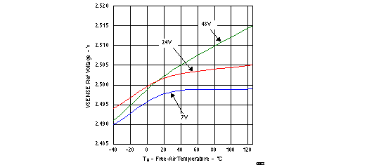
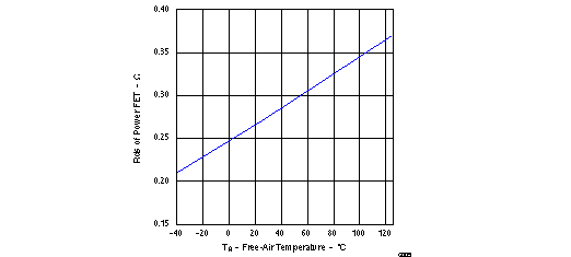
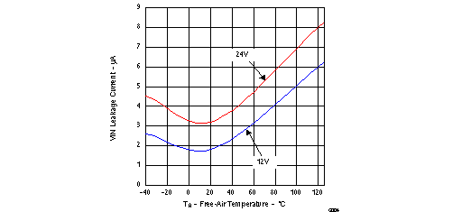
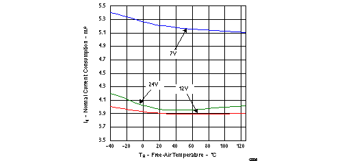
6.6 Typical Characteristics