SLVSCW4B April 2016 – May 2019 TPS560200-Q1
PRODUCTION DATA.
- 1 Features
- 2 Applications
- 3 Description
- 4 Revision History
- 5 Pin Configuration and Functions
- 6 Specifications
- 7 Detailed Description
- 8 Application and Implementation
- 9 Power Supply Recommendations
- 10Layout
- 11Device and Documentation Support
- 12Mechanical, Packaging, and Orderable Information
Package Options
Mechanical Data (Package|Pins)
- DGK|8
Thermal pad, mechanical data (Package|Pins)
- DGK|8
Orderable Information
8.2.3 Application Curves
VIN = 12 V, VOUT = 1.05 V, TA = 25°C (unless otherwise noted).
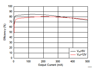 Figure 8. Efficiency
 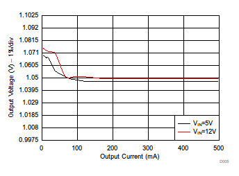 Figure 10. Load Regulation
 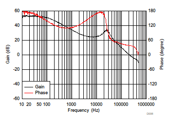 Figure 12. Loop Response, IOUT = 0.25 A
 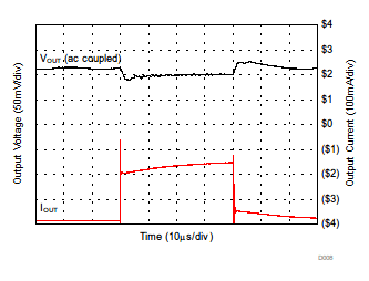 Figure 14. Transient Response, 2% to 50% Load Step
 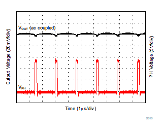 Figure 16. Output Ripple, IOUT = 500 mA
 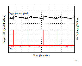 Figure 18. Output Ripple, IOUT = 0 mA
 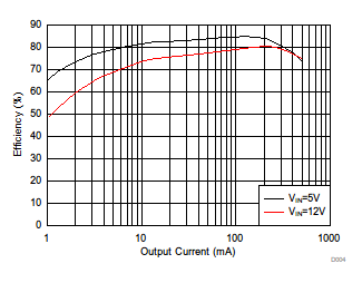 Figure 9. Light-Load Efficiency
 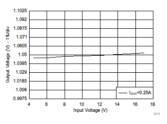 Figure 11. Line Regulation
 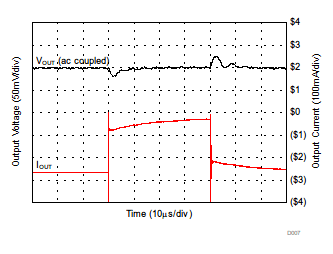 Figure 13. Transient Response, 25% to 75% Load Step
 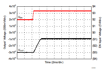 Figure 15. Start-Up Relative to EN
 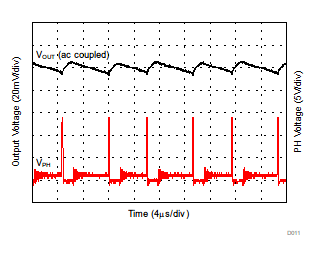 Figure 17. Output Ripple, IOUT = 30 mA