SLVSCB0E january   2014  – may 2023 TPS562200 , TPS563200

PRODUCTION DATA  

  1. Features
  2. Applications
  3. Description
  4. Revision History
  5. Pin Configuration and Functions
  6. Specifications
    1. 6.1 Absolute Maximum Ratings #GUID-10807E29-2FD4-4A3F-94B2-FDEBD147A133/SLVSC819633
    2. 6.2 ESD Ratings
    3. 6.3 Recommended Operating Conditions
    4. 6.4 Thermal Information
    5. 6.5 Electrical Characteristics
    6. 6.6 Timing Requirements
    7. 6.7 Typical Characteristics TPS562200
    8. 6.8 Typical Characteristics TPS563200
  7. Detailed Description
    1. 7.1 Overview
    2. 7.2 Functional Block Diagram
    3. 7.3 Feature Description
      1. 7.3.1 The Adaptive On-Time Control And PWM Operation
      2. 7.3.2 Advanced Eco-mode Control
      3. 7.3.3 Soft Start And Pre-Biased Soft Start
      4. 7.3.4 Current Protection
      5. 7.3.5 Over Voltage Protection
      6. 7.3.6 UVLO Protection
      7. 7.3.7 Thermal Shutdown
    4. 7.4 Device Functional Modes
      1. 7.4.1 Normal Operation
      2. 7.4.2 Eco-mode Operation
      3. 7.4.3 Standby Operation
  8. Application and Implementation
    1. 8.1 Application Information
    2. 8.2 Typical Applications
      1. 8.2.1 Tps562200 4.5-V To 17-V Input, 1.05-V Output Converter
        1. 8.2.1.1 Design Requirements
        2. 8.2.1.2 Detailed Design Procedures
          1. 8.2.1.2.1 Custom Design with WEBENCH® Tools
          2. 8.2.1.2.2 Output Voltage Resistors Selection
          3. 8.2.1.2.3 Output Filter Selection
          4. 8.2.1.2.4 Input Capacitor Selection
          5. 8.2.1.2.5 Bootstrap Capacitor Selection
        3. 8.2.1.3 Application Curves
      2. 8.2.2 Tps563200 4.5-V To 17-V Input, 1.05-V Output Converter
        1. 8.2.2.1 Design Requirements
        2. 8.2.2.2 Detailed Design Procedures
          1. 8.2.2.2.1 Output Filter Selection
        3. 8.2.2.3 Application Curves
    3. 8.3 Power Supply Recommendations
    4. 8.4 Layout
      1. 8.4.1 Layout Guidelines
      2. 8.4.2 Layout Example
  9. Device and Documentation Support
    1. 9.1 Device Support
      1. 9.1.1 Development Support
        1. 9.1.1.1 Custom Design with WEBENCH® Tools
    2. 9.2 Receiving Notification of Documentation Updates
    3. 9.3 Support Resources
    4. 9.4 Trademarks
    5. 9.5 Electrostatic Discharge Caution
    6. 9.6 Glossary
  10. 10Mechanical, Packaging, And Orderable Information

Package Options

Mechanical Data (Package|Pins)
Thermal pad, mechanical data (Package|Pins)
Orderable Information

Description

The TPS562200 and TPS563200 are simple, easy-to-use, 2-A and 3-A synchronous step-down (buck) converters in 6-pin SOT-23 package.

The devices are optimized to operate with minimum external component counts and also optimized to achieve low standby current.

These switch mode power supply (SMPS) devices employ D-CAP2 control topology providing a fast transient response and supporting both low equivalent series resistance (ESR) output capacitors such as specialty polymer and ultra-low ESR ceramic capacitors with no external compensation components.

TPS562200 and TPS563200 operate in Advanced Eco-mode, which maintains high efficiency during light load operation. The devices are available in a 6-pin 1.6-mm × 2.9-mm SOT (DDC) package, and specified from –40°C to 85°C of ambient temperature.

Device Information(1)
PART NUMBEROutput Current (Max)Package
TPS5622002 ADRL (SOT-236, 6)
TPS563200 3 A
For all available packages, see the orderable addendum at the end of the data sheet.
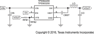
GUID-077A5829-48D9-4562-8A11-148676F40ED6-low.gifSimplified Schematic
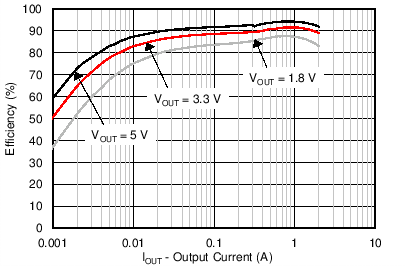
GUID-76550751-A8F8-40AE-8C0B-C816A4AA2019-low.pngTps562200 Efficiency