SLVSDU7 January 2017 TPS568215OA
PRODUCTION DATA.
- 1 Features
- 2 Applications
- 3 Description
- 4 Revision History
- 5 Pin Configuration and Functions
- 6 Specifications
-
7 Detailed Description
- 7.1 Overview
- 7.2 Functional Block Diagram
- 7.3
Feature Description
- 7.3.1 PWM Operation and D-CAP3 Control
- 7.3.2 Out-of-Audio Operation
- 7.3.3 4.7 V LDO and External Bias
- 7.3.4 MODE Selection
- 7.3.5 Soft Start and Pre-biased Soft Start
- 7.3.6 Enable and Adjustable UVLO
- 7.3.7 Power Good
- 7.3.8 Over Current Protection and Under Voltage Protection
- 7.3.9 Out-of-Bounds Operation
- 7.3.10 UVLO Protection
- 7.3.11 Thermal Shutdown
- 7.3.12 Output Voltage Discharge
- 7.4 Device Functional Modes
- 8 Application and Implementation
- 9 Power Supply Recommendations
- 10Layout
- 11Device and Documentation Support
- 12Mechanical, Packaging, and Orderable Information
Package Options
Mechanical Data (Package|Pins)
- RNN|18
Thermal pad, mechanical data (Package|Pins)
Orderable Information
1 Features
- Integrated 19-mΩ and 9.4-mΩ MOSFETs
- Selectable FSW of 400 kHz, 800 kHz or 1.2 MHz
- Out-of-Audio Feature to Keep Switching Frequency Out of Audio Frequency Range
- Adjustable Current Limit Settings with Hiccup Re-start
- 0.6 V ±1% Reference Voltage Across Full Temperature Range
- Optional External 5-V Bias Support for Enhanced Efficiency
- D-CAP3™ Control Mode for Fast Transient Response
- 0.6 V to 5.5 V Output Voltage Range
- Supports all Ceramic Capacitors
- Monotonic Startup into Pre-biased Outputs
- Adjustable Soft Start with a Default 1-ms Soft Start Time
- –40°C to 150°C Operating Junction Temperature
- Small 3.5-mm x 3.5-mm HotRod™ QFN Package
2 Applications
- Server and Storage
- Set top Box, High-End DTV
- Laptop and Gaming Systems
3 Description
The TPS568215OA is TI's smallest monolithic 8-A synchronous buck converter with an adaptive on-time D-CAP3™ control mode. The device integrates low RDS(on) power MOSFETs that enable high efficiency and it offers ease-of-use with minimal external component count for space-conscious power systems. Key features include a very accurate reference voltage, fast load transient response, Out-of-Audio mode, adjustable current limit and no requirement for external compensation. A forced continuous conduction mode helps meet tight voltage regulation accuracy requirements for performance DSPs and FPGAs. The TPS568215OA is available in a thermally enhanced 18-pin HotRod™ QFN package and is designed to operate from –40°C to 150°C junction temperature. TPS568215OA is pin to pin compatible with TPS568215 and TPS56C215 which gives the user flexibility to pick solutions from 6A to 12A in the same footprint.
Device Information(1)
| PART NUMBER | PACKAGE | BODY SIZE (NOM) |
|---|---|---|
| TPS568215OA | VQFN (18) | 3.50 mm x 3.50 mm |
- For all available packages, see the orderable addendum at the end of the data sheet.
spacer
spacer
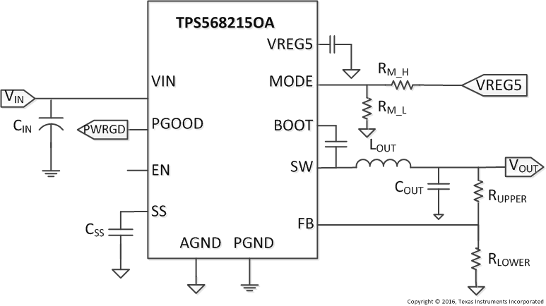
Typical Application Schematic

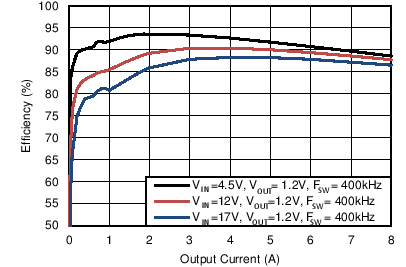
Efficiency vs Output Current
