SLVSDU7 January 2017 TPS568215OA
PRODUCTION DATA.
- 1 Features
- 2 Applications
- 3 Description
- 4 Revision History
- 5 Pin Configuration and Functions
- 6 Specifications
-
7 Detailed Description
- 7.1 Overview
- 7.2 Functional Block Diagram
- 7.3
Feature Description
- 7.3.1 PWM Operation and D-CAP3 Control
- 7.3.2 Out-of-Audio Operation
- 7.3.3 4.7 V LDO and External Bias
- 7.3.4 MODE Selection
- 7.3.5 Soft Start and Pre-biased Soft Start
- 7.3.6 Enable and Adjustable UVLO
- 7.3.7 Power Good
- 7.3.8 Over Current Protection and Under Voltage Protection
- 7.3.9 Out-of-Bounds Operation
- 7.3.10 UVLO Protection
- 7.3.11 Thermal Shutdown
- 7.3.12 Output Voltage Discharge
- 7.4 Device Functional Modes
- 8 Application and Implementation
- 9 Power Supply Recommendations
- 10Layout
- 11Device and Documentation Support
- 12Mechanical, Packaging, and Orderable Information
Package Options
Mechanical Data (Package|Pins)
- RNN|18
Thermal pad, mechanical data (Package|Pins)
Orderable Information
8 Application and Implementation
NOTE
Information in the following applications sections is not part of the TI component specification, and TI does not warrant its accuracy or completeness. TI’s customers are responsible for determining suitability of components for their purposes. Customers should validate and test their design implementation to confirm system functionality.
8.1 Application Information
The schematic of Figure 22 shows a typical application for TPS568215OA. This design converts an input voltage range of 4.5 V to 17 V down to 1.2 V with a maximum output current of 10 A.
8.2 Typical Application
 Figure 22. Application Schematic
8.2.1 Design Requirements
Table 4. Design Parameters
| PARAMETER | CONDITIONS | MIN | TYP | MAX | UNIT | |
|---|---|---|---|---|---|---|
| VOUT | Output voltage | 1.2 | V | |||
| IOUT | Output current | 10 | A | |||
| ΔVOUT | Transient response | 4-A load step | ±30 | mV | ||
| VIN | Input voltage | 4.5 | 12 | 17 | V | |
| VOUT(ripple) | Output voltage ripple | <10 | mV(P-P) | |||
| Start input voltage | Input voltage rising | Internal UVLO | V | |||
| Stop input voltage | Input voltage falling | Internal UVLO | V | |||
| fSW | Switching frequency | 1.2 | MHz | |||
| Operating Mode | OOA | |||||
| TA | Ambient temperature | 25 | °C | |||
8.2.2 Detailed Design Procedure
8.2.2.1 External Component Selection
8.2.2.1.1 Output Voltage Set Point
To change the output voltage of the application, it is necessary to change the value of the upper feedback resistor. By changing this resistor the user can change the output voltage above 0.6 V. See Equation 5

8.2.2.1.2 Switching Frequency and Mode Selection
Switching Frequency, current limit and switching mode (OOA or FCCM) are set by a voltage divider from VREG5 to GND connected to the MODE pin. See Table 3 for possible MODE pin configurations. Switching frequency selection is a tradeoff between higher efficiency and smaller system solution size. Lower switching frequency yields higher overall efficiency but relatively bigger external components. Higher switching frequencies cause additional switching losses which impact efficiency and thermal performance. For this design 1.2 MHz is chosen as the switching frequency, the switching mode is OOA and the output current is 8 A.
8.2.2.1.3 Inductor Selection
The inductor ripple current is filtered by the output capacitor. A higher inductor ripple current means the output capacitor should have a ripple current rating higher than the inductor ripple current. See Table 5 for recommended inductor values.
The RMS and peak currents through the inductor can be calculated using Equation 6 and Equation 7. It is important that the inductor is rated to handle these currents.


During transient/short circuit conditions the inductor current can increase up to the current limit of the device so it is safe to choose an inductor with a saturation current higher than the peak current under current limit condition.
8.2.2.1.4 Output Capacitor Selection
After selecting the inductor the output capacitor needs to be optimized. In DCAP3, the regulator reacts within one cycle to the change in the duty cycle so the good transient performance can be achieved without needing large amounts of output capacitance. The recommended output capacitance range is given in Table 5
Ceramic capacitors have very low ESR, otherwise the maximum ESR of the capacitor should be less than VOUT(ripple)/IOUT(ripple)
Table 5. Recommended Component Values
| VOUT (V) | RLOWER (kΩ) | RUPPER (kΩ) | FSW (kHz) | LOUT (µH) | COUT(min) (µF) | COUT(max) (µF) | CFF (pF) |
|---|---|---|---|---|---|---|---|
| 0.6 | 10 | 0 | 400 | 0.68 | 300 | 500 | – |
| 800 | 0.47 | 100 | 500 | – | |||
| 1200 | 0.33 | 88 | 500 | – | |||
| 1.2 | 10 | 400 | 1.2 | 100 | 500 | – | |
| 800 | 0.68 | 88 | 500 | – | |||
| 1200 | 0.47 | 88 | 500 | – | |||
| 3.3 | 45.3 | 400 | 2.4 | 88 | 500 | 100–220 | |
| 800 | 1.5 | 88 | 500 | 100–220 | |||
| 1200 | 1.1 | 88 | 500 | 100–220 | |||
| 5.5 | 82.5 | 400 | 3.3 | 88 | 500 | 100–220 | |
| 800 | 2.4 | 88 | 500 | 100–220 | |||
| 1200 | 1.2 | 88 | 700 | 100–220 |
8.2.2.1.5 Input Capacitor Selection
The minimum input capacitance required is given in Equation 8.

TI recommends using a high quality X5R or X7R input decoupling capacitors of 40 µF on the input voltage pin. The voltage rating on the input capacitor must be greater than the maximum input voltage. The capacitor must also have a ripple current rating greater than the maximum input current ripple of the application. The input ripple current is calculated by Equation 9 below:

8.2.3 Application Curves
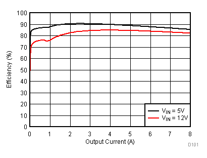
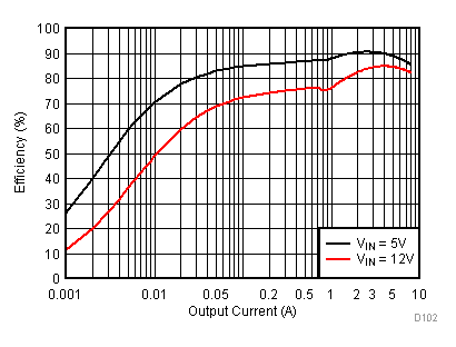
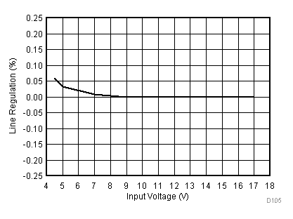
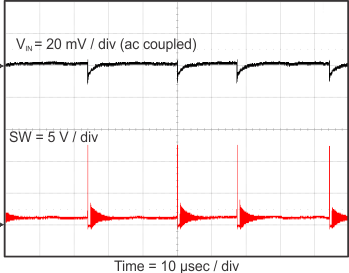
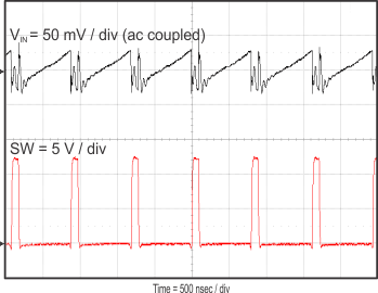
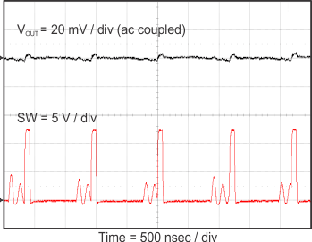
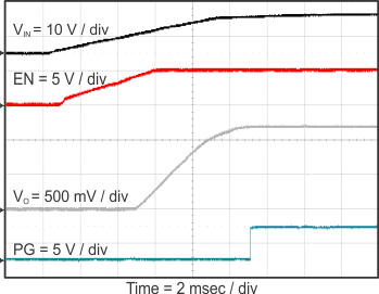
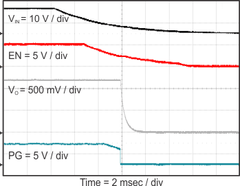
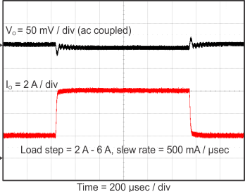
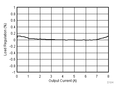
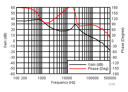
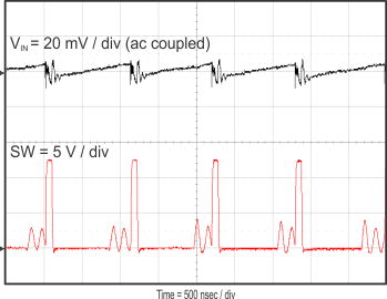
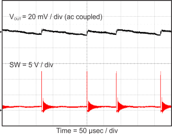
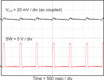
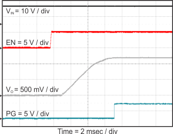
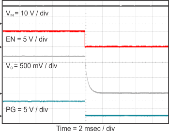
Figure 23 through Figure 39 apply to the circuit of Figure 22. VIN = 12 V. Ta = 25 °C unless otherwise specified.
