SLVSDU7 January 2017 TPS568215OA
PRODUCTION DATA.
- 1 Features
- 2 Applications
- 3 Description
- 4 Revision History
- 5 Pin Configuration and Functions
- 6 Specifications
-
7 Detailed Description
- 7.1 Overview
- 7.2 Functional Block Diagram
- 7.3
Feature Description
- 7.3.1 PWM Operation and D-CAP3 Control
- 7.3.2 Out-of-Audio Operation
- 7.3.3 4.7 V LDO and External Bias
- 7.3.4 MODE Selection
- 7.3.5 Soft Start and Pre-biased Soft Start
- 7.3.6 Enable and Adjustable UVLO
- 7.3.7 Power Good
- 7.3.8 Over Current Protection and Under Voltage Protection
- 7.3.9 Out-of-Bounds Operation
- 7.3.10 UVLO Protection
- 7.3.11 Thermal Shutdown
- 7.3.12 Output Voltage Discharge
- 7.4 Device Functional Modes
- 8 Application and Implementation
- 9 Power Supply Recommendations
- 10Layout
- 11Device and Documentation Support
- 12Mechanical, Packaging, and Orderable Information
Package Options
Mechanical Data (Package|Pins)
- RNN|18
Thermal pad, mechanical data (Package|Pins)
Orderable Information
10 Layout
10.1 Layout Guidelines
- Recommend a four-layer or six-layer PCB for good thermal performance and with maximum ground plane. 3" x 3", four-layer PCB with 2-oz. copper used as example.
- Recommend having equal caps on each side of the IC. Place them right across VIN as close as possible.
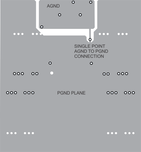
- Inner layer 1 will be ground with the PGND to AGND net tie
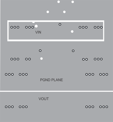
- Inner layer2 has VIN copper pour that has vias to the top layer VIN. Place multiple vias under the device near VIN and GND and near input capacitors to reduce parasitic inductance and improve thermal performance
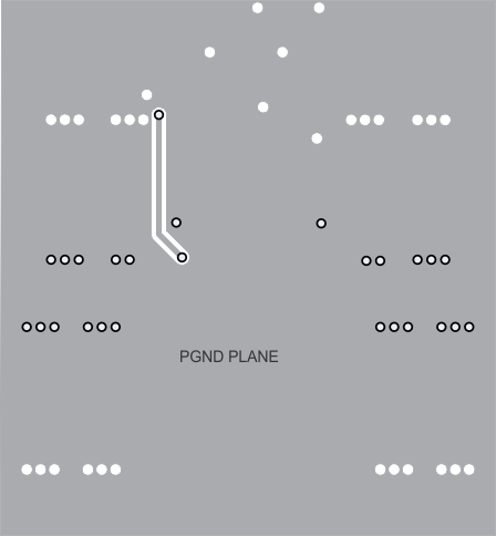
- Bottom later is GND with the BOOT trace routing.
- Feedback should be referenced to the quite AGND and routed away from the switch node.
- VIN trace must be wide to reduce the trace impedance.
10.2 Layout Example
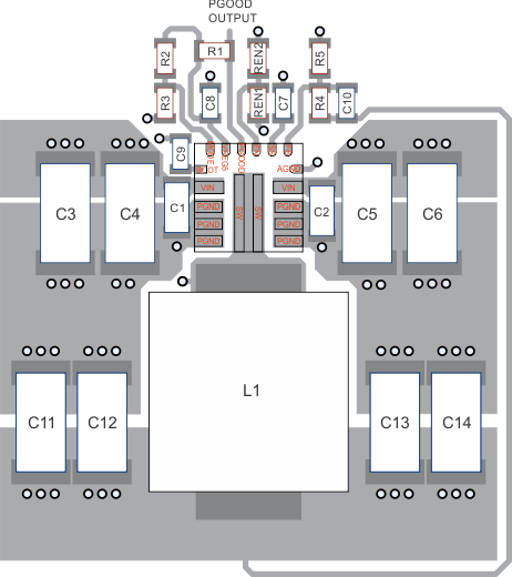
Figure 40 shows the recommended top side layout. Component reference designators are the same as the circuit shown in Figure 22. Resistor divider for EN is not used in the circuit of Figure 22, but are shown in the layout for reference.
 Figure 40. Top Side Layout
Figure 41 shows the recommended layout for the first internal layer. It is comprised of a large PGND plane and a smaller ANGD island. AGND and PGND are connected at a single point to reduce circulating currents.
 Figure 41. Mid Layer 1 Layout
Figure 42 shows the recommended layout for the second internal layer. It is comprised of a large PGND plane, a smaller copper fill area to connect the two top side VIN copper areas and a second VOUT copper fill area.
 Figure 42. Mid Layer 2 Layout
Figure 43 shows the recommended layout for the bottom layer. It is comprised of a large PGND plane and a trace to connect the BOOT capacitor to the SW node.
 Figure 43. Bottom Layer Layout