SLVSDU7 January 2017 TPS568215OA
PRODUCTION DATA.
- 1 Features
- 2 Applications
- 3 Description
- 4 Revision History
- 5 Pin Configuration and Functions
- 6 Specifications
-
7 Detailed Description
- 7.1 Overview
- 7.2 Functional Block Diagram
- 7.3
Feature Description
- 7.3.1 PWM Operation and D-CAP3 Control
- 7.3.2 Out-of-Audio Operation
- 7.3.3 4.7 V LDO and External Bias
- 7.3.4 MODE Selection
- 7.3.5 Soft Start and Pre-biased Soft Start
- 7.3.6 Enable and Adjustable UVLO
- 7.3.7 Power Good
- 7.3.8 Over Current Protection and Under Voltage Protection
- 7.3.9 Out-of-Bounds Operation
- 7.3.10 UVLO Protection
- 7.3.11 Thermal Shutdown
- 7.3.12 Output Voltage Discharge
- 7.4 Device Functional Modes
- 8 Application and Implementation
- 9 Power Supply Recommendations
- 10Layout
- 11Device and Documentation Support
- 12Mechanical, Packaging, and Orderable Information
Package Options
Mechanical Data (Package|Pins)
- RNN|18
Thermal pad, mechanical data (Package|Pins)
Orderable Information
7 Detailed Description
7.1 Overview
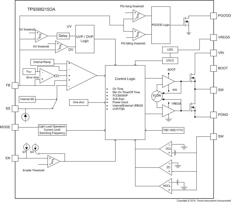
The TPS568215OA is a high density synchronous step down buck converter which can operate from 4.5-V to 17-V input voltage (VIN). It has 19-mΩ and 9-mΩ integrated MOSFETs that enable high efficiency up to 10 A. The device employs D-CAP3™ mode control that provides fast transient response with no external compensation components and an accurate feedback voltage. The control topology provides seamless transition between FCCM operating mode at higher load condition and OOA operation at lighter load condition. OOA feature allows the TPS568215OA to keep switching frequency above the audible frequency range. The TPS568215OA is able to adapt to both low equivalent series resistance (ESR) output capacitors such as POSCAP or SP-CAP, and ultralow ESR ceramic capacitors.
The TPS568215OA has three selectable switching frequencies (FSW) 400kHz, 800kHz and 1200kHz which gives the flexibility to optimize the design for higher efficiency or smaller size. There are three selectable current limits. All these options are configured by choosing the right voltage on the MODE pin.
The TPS568215OA has a 4.7 V internal LDO that creates bias for all internal circuitry. There is a feature to overdrive this internal LDO with an external voltage on the VREG5 pin which improves the converter’s efficiency. The undervoltage lockout (UVLO) circuit monitors the VREG5 pin voltage to protect the internal circuitry from low input voltages. The device has an internal pull-up current source on the EN pin which can enable the device even with the pin floating.
Soft-start time can be selected by connecting a capacitor to the SS pin. The device is protected from output short, undervoltage and over temperature conditions.
7.2 Functional Block Diagram

7.3 Feature Description
7.3.1 PWM Operation and D-CAP3™ Control
The TPS568215OA operates using the adaptive on-time PWM control with a proprietary D-CAP3™ control which enables low external component count with a fast load transient response while maintaining a good output voltage accuracy. At the beginning of each switching cycle the high side MOSFET is turned on for an on-time set by an internal one shot timer. This on-time is set based on the converter’s input voltage, output voltage and the pseudo-fixed frequency hence this type of control topology is called an adaptive on-time control. The one shot timer resets and turns on again once the feedback voltage (VFB) falls below the internal reference voltage (VREF). An internal ramp is generated which is fed to the FB pin to simulate the output voltage ripple. This enables the use of very low-ESR output capacitors such as multi-layered ceramic caps (MLCC). No external current sense network or loop compensation is required for DCAP3™ control topology.
The TPS568215OA includes an error amplifier that makes the output voltage very accurate. This error amplifier is absent in other flavors of DCAP3™. For any control topology that is compensated internally, there is a range of the output filter it can support. The output filter used with the TPS568215OA is a low pass L-C circuit. This L-C filter has double pole that is described in

At low frequencies, the overall loop gain is set by the output set-point resistor divider network and the internal gain of the TPS568215OA. The low frequency L-C double pole has a 180 degree in phase. At the output filter frequency, the gain rolls off at a –40dB per decade rate and the phase drops rapidly. The internal ripple generation network introduces a high-frequency zero that reduces the gain roll off from –40dB to –20dB per decade and increases the phase to 90 degree one decade above the zero frequency. The internal ripple injection high frequency zero is changed according to the switching frequency selected as shown in table below. The inductor and capacitor selected for the output filter must be such that the double pole is located close enough to the high-frequency zero so that the phase boost provided by this high-frequency zero provides adequate phase margin for the stability requirement. The crossover frequency of the overall system should usually be targeted to be less than one-fifth of the switching frequency (FSW).
Table 1. Ripple Injection Zero
| SWITCHING FREQUENCY (kHz) | ZERO LOCATION (kHz) |
|---|---|
| 400 | 7.1 |
| 800 | 14.3 |
| 1200 | 21.4 |
Table 2 lists the inductor values and part numbers that are used to plot the efficiency curves in the Typical Characteristics section.
Table 2. Inductor Values
| VOUT(V) | FSW(kHz) | LOUT(uH) | Würth PART NUMBER(1) |
|---|---|---|---|
| 1.2 | 400 | 1.2 | 744325120 |
| 800 | 0.68 | 744311068 | |
| 1200 | 0.47 | 744314047 | |
| 3.3 | 400 | 2.4 | 744325240 |
| 800 | 1.5 | 744314150 | |
| 1200 | 1.1 | 744314110 | |
| 5.5 | 400 | 3.3 | 744325330 |
| 800 | 2.4 | 744325240 | |
| 1200 | 1.2 | 744325120 |
7.3.2 Out-of-Audio Operation™
The TPS568215OA is designed with OOA feature that keeps switching frequency above the audible frequency region at light load or no load conditions. Once the converter determines that there is no switching for longer than 40us, it turns on the LS FET which brings VFB lower than internal VREF and initiates a new Ton cycle. This ensures that the switching frequency doesn’t go lower than 25kHz typical.
7.3.3 4.7 V LDO and External Bias
The VREG5 pin is the output of the internal 4.7-V linear regulator that creates the bias for all the internal circuitry and MOSFET gate drivers. The VREG5 pin needs to be bypassed with a 4.7-µF capacitor. An external voltage that is above the LDO's internal output voltage can override the internal LDO, switching it to the external rail once a higher voltage is detected. This enhances the efficiency of the converter because the quiescent current now runs off this external rail instead of the input power supply. The UVLO circuit monitors the VREG5 pin voltage and disables the output when VREG5 falls below the UVLO threshold. When using an external bias on the VREG5 rail, any power-up and power-down sequencing can be applied but it is important to understand that if there is a discharge path on the VREG5 rail that can pull a current higher than the internal LDO's current limit (ILIM5) from the VREG5, then the VREG5 LDO turns off thereby shutting down the output of TPS568215OA. If such condition does not exist and if the external VREG5 rail is turned off, the VREG5 voltage switches over to the internal LDO voltage which is 4.7 V typically in a few nanoseconds. Figure 26 below shows this transition of the VREG5 voltage from an external bias of 5.5 V to the internal LDO output of 4.7 V when the external bias to VREG5 is disabled while the output of TPS568215OA remains unchanged.
7.3.4 MODE Selection
TPS568215OA has a MODE pin that can offer 16 different states of operation as a combination of Current Limit, Switching Frequency and Light Load operation. The device can operate at three different current limits ILIM-1,ILIM and ILIM+1 to support an output continuous current of 6 A, 8 A and 10A respectively. the device can provide 10A output current only at switching frequencies of 400kHz and 800kHz.The TPS568215OA is designed to compare the valley current of the inductor against the current limit thresholds so it is important to understand that the output current will be half the ripple current above the valley current. TPS568215OA can operate at three different frequencies of 400 kHz, 800 kHz and 1200 kHz and also can choose between OOA and FCCM mode. The device reads the voltage on the MODE pin during start-up and latches onto one of the MODE options listed below in table 3. The voltage on the MODE pin can be set by connecting this pin to the center tap of a resistor divider connected between VREG5 and AGND. A guideline for the top resistor (RM_H) and the bottom resistor (RM_L) as 5% resistors is shown in Table 3. It is important that the voltage for the MODE pin is derived from the VREG5 rail only since internally this voltage is referenced to detect the MODE option. The MODE pin setting can be reset only by a VIN power cycling.
Table 3. Mode Pin Resistor Settings
| RM_L (kΩ) | RM_H (kΩ) | LIGHT LOAD OPERATION | CURRENT LIMIT | FREQUENCY (kHz) |
| 5.1 | 300 | FCCM | ILIM-1 | 400 |
| 10 | 200 | FCCM | ILIM | 400 |
| 20 | 240 | FCCM | ILIM+1 | 400 |
| 20 | 160 | FCCM | ILIM-1 | 800 |
| 20 | 120 | FCCM | ILIM | 800 |
| 51 | 240 | FCCM | ILIM+1 | 800 |
| 51 | 200 | FCCM | ILIM-1 | 1200 |
| 51 | 180 | FCCM | ILIM | 1200 |
| 51 | 150 | OOA | ILIM-1 | 400 |
| 51 | 120 | OOA | ILIM | 400 |
| 51 | 110 | OOA | ILIM+1 | 400 |
| 51 | 91 | OOA | ILIM-1 | 800 |
| 51 | 82 | OOA | ILIM | 800 |
| 51 | 75 | OOA | ILIM+1 | 800 |
| 51 | 62 | OOA | ILIM-1 | 1200 |
| 51 | 51 | OOA | ILIM | 1200 |
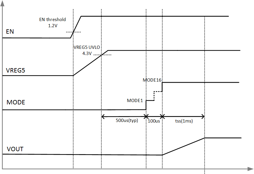
Figure 20 below shows the typical start-up sequence of the device once the enable signal crosses the EN turn-on threshold. After the voltage on VREG5 crosses the rising UVLO threshold it takes about 500us to read the first mode setting and approximately 100us from there to finish the last mode setting. The output voltage starts ramping after the mode reading is done.
 Figure 20. Power-Up Sequence
7.3.5 Soft Start and Pre-biased Soft Start
The TPS568215OA has an adjustable soft-start time that can be set by connecting a capacitor on SS pin. When the EN pin becomes high, the soft-start charge current (ISS) begins charging the external capacitor (CSS) connected between SS and AGND. The devices tracks the lower of the internal soft-start voltage or the external soft-start voltage as the reference. The equation for the soft-start time (TSS) is shown in Equation 2:

where
- VREF is 0.6 V and ISS is 6 µA
If the output capacitor is pre-biased at startup, the device initiates switching and starts ramping up only after the internal reference voltage becomes greater than the feedback voltage VFB. This scheme ensures that the converters ramp up smoothly into regulation point.
7.3.6 Enable and Adjustable UVLO
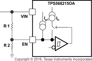
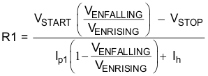
The EN pin controls the turn-on and turn-off of the device. When EN pin voltage is above the turn-on threshold which is around 1.2 V, the device starts switching and when the EN pin voltage falls below the turn-off threshold which is around 1.1V it stops switching. If the user application requires a different turn-on (VSTART) and turn-off thresholds (VSTOP) respectively, the EN pin can be configured as shown in Figure 21 by connecting a resistor divider between VIN and EN. The EN pin has a pull-up current Ip1 that sets the default state of the pin when it is floating. This current increases to Ip2 when the EN pin voltage crosses the turn-on threshold. The UVLO thresholds can be set by using Equation 3 and Equation 4.
 Figure 21. Adjustable VIN Under Voltage Lock Out


where
- Ip2 = 4.197 μA
- Ip1 = 1.91 μA
- Ih = 2.287 μA
- VENRISING = 1.225 V
- VENFALLING = 1.104 V
7.3.7 Power Good
The Power Good (PGOOD) pin is an open drain output. Once the FB pin voltage is between 93% and 107% of the internal reference voltage (VREF) the PGOOD is de-asserted and floats after a 200 μs de-glitch time. A pull-up resistor of 10 kΩ is recommended to pull it up to VREG5. The PGOOD pin is pulled low when the FB pin voltage is lower than VUVP or greater than VOVP threshold; or, in an event of thermal shutdown or during the soft-start period.
7.3.8 Over Current Protection and Under Voltage Protection
The output overcurrent limit (OCL) is implemented using a cycle-by-cycle valley detect control circuit. The switch current is monitored during the OFF state by measuring the low-side FET drain to source voltage. This voltage is proportional to the switch current. During the on time of the high-side FET switch, the switch current increases at a linear rate determined by input voltage , output voltage, the on-time and the output inductor value. During the on time of the low-side FET switch, this current decreases linearly. The average value of the switch current is the load current IOUT. If the measured drain to source voltage of the low-side FET is above the voltage proportional to current limit, the low side FET stays on until the current level becomes lower than the OCL level which reduces the output current available. When the current is limited the output voltage tends to drop because the load demand is higher than what the converter can support. When the output voltage falls below 68% of the target voltage, the UVP comparator detects it and shuts down the device after a wait time of 1ms, the device re-starts after a hiccup time of 7ms. In this type of valley detect control the load current is higher than the OCL threshold by one half of the peak to peak inductor ripple current. When the overcurrent condition is removed, the output voltage returns to the regulated value. If an OCL condition happens during start-up then the device enters hiccup-mode immediately without a wait time of 1ms.
7.3.9 Out-of-Bounds Operation
The device has an out-of-bounds (OOB) overvoltage protection that protects the output load at a much lower overvoltage threshold of 8% above the target voltage. OOB protection does not trigger an overvoltage fault, OOB protection operates as an early no-fault overvoltage protection mechanism. During the OOB operation, the controller operates in forced PWM mode only by turning on the low-side FET. Turning on the low-side FET beyond the zero inductor current quickly discharges the output capacitor thus causing the output voltage to fall quickly toward the setpoint. During the operation, the cycle-by cycle negative current limit is also activated to ensure the safe operation of the internal FETs.
7.3.10 UVLO Protection
Under voltage lock out protection (UVLO) monitors the internal VREG5 regulator voltage. When the VREG5 voltage is lower than UVLO threshold voltage, the device is shut off. This protection is non-latching.
7.3.11 Thermal Shutdown
The device monitors the internal die temperature. If this temperature exceeds the thermal shutdown threshold value (TSDN typically 160°C) the device shuts off. This is a non-latch protection. During start up, if the device temperature is higher than 160°C the device does not start switching and does not load the MODE settings. If the device temp goes higher than TSDN threshold after startup, it stops switching with SS reset to ground and an internal discharge switch turns on to quickly discharge the output voltage. The device re-starts switching when the temperature goes below the thermal shutdown threshold but the MODE settings are not re-loaded again. There is a second higher thermal protection on the device TSDN VREG5 which protects it from over temperature conditions not caused by the switching of the device itself. This threshold is at typically 170°C. Even under nonswitching condition of the device after exceeding TSDN threshold, if it still continues to heat up the VREG5 output shuts off once temperature goes beyond TSDN VREG5, thereby shutting down the device completely.
7.3.12 Output Voltage Discharge
The device has a 500ohm discharge switch that discharges the output VOUT through SW node during any event of fault like output overvoltage, output undervoltage , TSD , if VREG5 voltage below the UVLO and when the EN pin voltage (VEN) is below the turn-on threshold.
7.4 Device Functional Modes
7.4.1 Light Load Operation
When the MODE pin is selected to operate in FCCM mode, the converter operates in continuous conduction mode (FCCM) during light-load conditions. During FCCM, the switching frequency (FSW) is maintained at an almost constant level over the entire load range which is suitable for applications requiring tight control of the switching frequency and output voltage ripple at the cost of lower efficiency under light load. If the MODE pin is selected to operate in OOA, the device enters pulse skip mode after the valley of the inductor ripple current crosses zero. The OOA mode maintains higher efficiency at light load with a lower switching frequency but this switching frequency is restricted to not go below 25kHz typical.
7.4.2 Standby Operation
The TPS568215OA can be placed in standby mode by pulling the EN pin low. The device operates with a shutdown current of 7uA when in standby condition.