SLVSGB5 August 2022 TPS56C231
PRODUCTION DATA
- 1 Features
- 2 Applications
- 3 Description
- 4 Revision History
- 5 Pin Configuration and Functions
- 6 Specifications
-
7 Detailed Description
- 7.1 Overview
- 7.2 Functional Block Diagram
- 7.3
Feature Description
- 7.3.1 PWM Operation and D-CAP3 Control Mode
- 7.3.2 Eco-mode Control
- 7.3.3 4.7-V LDO
- 7.3.4 MODE Selection
- 7.3.5 Soft Start and Prebiased Soft Start
- 7.3.6 Enable and Adjustable UVLO
- 7.3.7 Power Good
- 7.3.8 Overcurrent Protection and Undervoltage Protection
- 7.3.9 UVLO Protection
- 7.3.10 Thermal Shutdown
- 7.3.11 Output Voltage Discharge
- 7.4 Device Functional Modes
- 8 Application and Implementation
- 9 Device and Documentation Support
- 10Mechanical, Packaging, and Orderable Information
Package Options
Refer to the PDF data sheet for device specific package drawings
Mechanical Data (Package|Pins)
- RNN|18
Thermal pad, mechanical data (Package|Pins)
Orderable Information
7.3.1 PWM Operation and D-CAP3 Control Mode
The TPS56C231x operates using the adaptive on-time PWM control with a proprietary D-CAP3 control mode, which enables low external component count with a fast load transient response while maintaining a good output voltage accuracy. At the beginning of each switching cycle, the high-side MOSFET is turned on for an on time set by an internal one-shot timer. This on time is set based on the input voltage of the converter, output voltage of the converter, and the pseudo-fixed frequency, hence this type of control topology is called an adaptive on-time control. The one-shot timer resets and turns on again once the feedback voltage (VFB) falls below the internal reference voltage (VREF). An internal ramp is generated, which is fed to the FB pin to simulate the output voltage ripple, enabling the use of very low-ESR output capacitors such as multi-layered ceramic caps (MLCC). No external current sense network or loop compensation is required for D-CAP3 control mode topology.
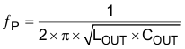
The TPS56C231x includes an error amplifier that makes the output voltage very accurate. This error amplifier is absent in other flavors of D-CAP3 control mode. For any control topology that is compensated internally, there is a range of the output filter it can support. The output filter used with the TPS56C231x is a low-pass L-C circuit. This L-C filter has double pole that is described in Equation 1.
At low frequencies, the overall loop gain is set by the output set-point resistor divider network and the internal gain of the TPS56C231x. The low frequency L-C double pole has a 180 degree in-phase. At the output filter frequency, the gain rolls off at a –40 dB per decade rate and the phase drops rapidly. The internal ripple generation network introduces a high-frequency zero that reduces the gain roll off from –40 dB to –20 dB per decade and increases the phase to 90 degree one decade above the zero frequency. The internal ripple injection high frequency zero is changed according to the switching frequency selected as shown in Table 7-1. The inductor and capacitor selected for the output filter must be such that the double pole is located close enough to the high-frequency zero so that the phase boost provided by this high-frequency zero provides adequate phase margin for the stability requirement. The crossover frequency of the overall system usually must be targeted to be less than one-fifth of the switching frequency (fSW).
| Switching Frequency (kHz) | Zero Location (kHz) |
|---|---|
| 400 | 17.8 |
| 800 | 27.1 |
| 1200 | 29.8 |