SLVSGB5 August 2022 TPS56C231
PRODUCTION DATA
- 1 Features
- 2 Applications
- 3 Description
- 4 Revision History
- 5 Pin Configuration and Functions
- 6 Specifications
-
7 Detailed Description
- 7.1 Overview
- 7.2 Functional Block Diagram
- 7.3
Feature Description
- 7.3.1 PWM Operation and D-CAP3 Control Mode
- 7.3.2 Eco-mode Control
- 7.3.3 4.7-V LDO
- 7.3.4 MODE Selection
- 7.3.5 Soft Start and Prebiased Soft Start
- 7.3.6 Enable and Adjustable UVLO
- 7.3.7 Power Good
- 7.3.8 Overcurrent Protection and Undervoltage Protection
- 7.3.9 UVLO Protection
- 7.3.10 Thermal Shutdown
- 7.3.11 Output Voltage Discharge
- 7.4 Device Functional Modes
- 8 Application and Implementation
- 9 Device and Documentation Support
- 10Mechanical, Packaging, and Orderable Information
Package Options
Refer to the PDF data sheet for device specific package drawings
Mechanical Data (Package|Pins)
- RNN|18
Thermal pad, mechanical data (Package|Pins)
Orderable Information
7.3.5 Soft Start and Prebiased Soft Start
The TPS56C231x has an internal 1.2-ms soft-start time and an external adjustable soft-start time that can be set by connecting a capacitor on the SS pin. When the EN pin becomes high, the soft-start charge current (ISS) begins charging the external capacitor (CSS) connected between SS and AGND. The device tracks the lower of the internal soft-start voltage or the external soft-start voltage as the reference. Equation 3 is the equation for the soft-start time (tSS):
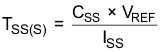
where
- VREF is 0.6 V and ISS is 6 µA.
If the output capacitor is prebiased at start-up, the device initiates switching and starts ramping up only after the internal reference voltage becomes greater than the feedback voltage, VFB. This scheme ensures that the converters ramp up smoothly into the regulation point.