SLVS258B November 1999 – December 2016 TPS60130 , TPS60131 , TPS60132 , TPS60133
PRODUCTION DATA.
- 1 Features
- 2 Applications
- 3 Description
- 4 Revision History
- 5 Device Options
- 6 Pin Configuration and Functions
- 7 Specifications
- 8 Parameter Measurement Information
- 9 Detailed Description
- 10Application and Implementation
- 11Power Supply Recommendations
- 12Layout
- 13Device and Documentation Support
- 14Mechanical, Packaging, and Orderable Information
Package Options
Mechanical Data (Package|Pins)
- PWP|20
Thermal pad, mechanical data (Package|Pins)
- PWP|20
Orderable Information
1 Features
- Up to 90% Efficiency From 2.7-V to 5.4-V Input Voltage Range Because of Special Switching Topology
- Up to 300-mA Output Current (TPS60130 and TPS60131)
- No Inductors Required, Low EMI
- Regulated 5-V ±4% Output
- Only Four External Components Required
- 60-µA Quiescent Supply Current
- 0.05-µA Shutdown Current
- Load Disconnected in Shutdown
- Thermally-Enhanced PowerPAD™ Package
2 Applications
- Battery-Powered Applications
- Three Battery Cells to 5-V Conversion or Point-of-Use 3.3-V to 5-V Conversion
- Lilon Battery to 5-V Conversion
- Portable Instruments
- Battery-Powered Microprocessor Systems
- Backup-Battery Boost Converters
- PDA’s, Organizers, Laptops
- Handheld Instrumentation
- Medical Instruments (for example, Glucose Meters)
- PCMCIA and 5-V Smart Card Supply
3 Description
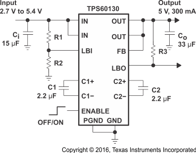
The TPS6013x step-up, regulated charge pump devices generate a 5-V ±4% output voltage from a 2.7-V to 5.4-V input voltage (three alkaline, NiCd, or NiMH batteries or one Lithium or Lilon battery). The output current is 300 mA for the TPS60130 and TPS60131, and 150 mA for the TPS60132 and TPS60133 devices, all from a 3-V input. Only four external capacitors are required to build a complete high efficiency dc/dc charge pump converter. To achieve the high efficiency over a wide input voltage range, the charge pump automatically selects between a 1.5× or doubler conversion mode. From a 3-V input, all ICs can start with full load current.
Device Information(1)
| PART NUMBER | PACKAGE | BODY SIZE (NOM) |
|---|---|---|
| TPS6013x | HTSSOP (20) | 6.50 mm × 4.40 mm |
- For all available packages, see the orderable addendum at the end of the data sheet.
Typical Operating Circuit

4 Revision History
Changes from A Revision (December 1999) to B Revision
- Added ESD Ratings table, Feature Description section, Device Functional Modes, Application and Implementation section, Power Supply Recommendations section, Layout section, Device and Documentation Support section, and Mechanical, Packaging, and Orderable Information section Go
- Deleted Lead temperature (260°C maximum) from Absolute Maximum Ratings tableGo