SLVS258B November 1999 – December 2016 TPS60130 , TPS60131 , TPS60132 , TPS60133
PRODUCTION DATA.
- 1 Features
- 2 Applications
- 3 Description
- 4 Revision History
- 5 Device Options
- 6 Pin Configuration and Functions
- 7 Specifications
- 8 Parameter Measurement Information
- 9 Detailed Description
- 10Application and Implementation
- 11Power Supply Recommendations
- 12Layout
- 13Device and Documentation Support
- 14Mechanical, Packaging, and Orderable Information
Package Options
Mechanical Data (Package|Pins)
- PWP|20
Thermal pad, mechanical data (Package|Pins)
- PWP|20
Orderable Information
9 Detailed Description
9.1 Overview
The TPS6013x charge pump devices provide a regulated 5-V output from a 2.7-V to 5.4-V input. They deliver a maximum load current of 300 mA or 150 mA (respectively). Designed specifically for space-critical, battery-powered applications, the complete charge pump circuit requires four external capacitors. The circuit is optimized for efficiency over a wide input voltage range.
9.2 Functional Block Diagram
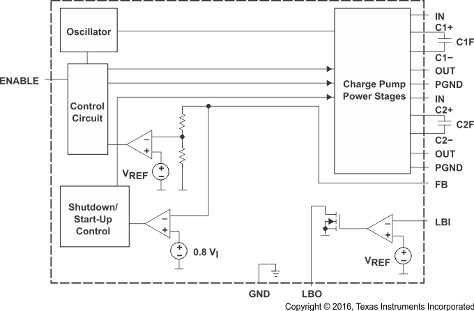
 Figure 19. TPS60130 and TPS60132 Block Diagram
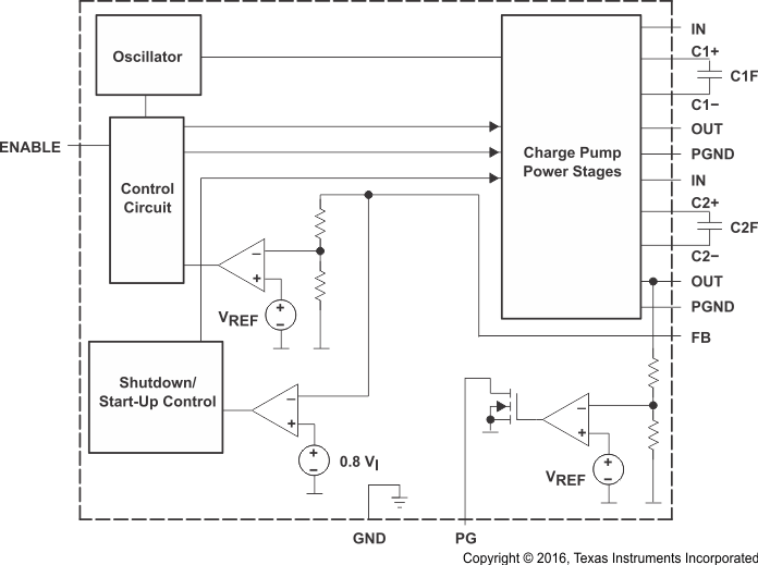
 Figure 20. TPS60131 and TPS60133 Block Diagram
9.3 Feature Description
9.3.1 Operating Principle
The TPS6013x charge pumps consist of an oscillator, a 1.21-V bandgap reference, an internal resistive feedback circuit, an error amplifier, high current MOSFET switches, a shutdown/startup circuit, a low battery or Power Good comparator, and a control circuit (see Figure 19 and Figure 20).
The device consists of two single-ended charge pumps. These charge pumps are automatically configured to amplify the input voltage with a conversion factor of 1.5 or 2. The conversion ratio is dependent on the input voltage and load current. This assures high efficiency over a wide input voltage range and is further described in Adaptive Mode Switching.
9.3.2 Adaptive Mode Switching
The ON-resistance of the MOSFETs that are in the charge path of the flying capacitors is regulated when the charge pump operates in voltage doubler mode. It is changed depending on the output voltage that is fed back into the control loop. This way, the time-constant during the charging phase can be modified and increased versus a time-constant for fully switched-on MOSFETs. The ON-resistance of both switches and the capacitance of the flying capacitor define the time constant. The MOSFET switches in the discharge path of the charge pump are always fully switched on to their minimum rDS(on). With the time-constant during charge phase being bigger than the time constant in discharge phase, the voltage on the flying capacitors stabilizes to the lowest possible value necessary to get a stable VO.
The voltage on the flying capacitors is measured and compared with the supply voltage VI. If the voltage across the flying capacitors is smaller than half of the supply voltage, then the charge pump switches into the 1.5× conversion-mode. The charge pump switches back from a 1.5× conversion-mode to a voltage doubler mode if the load current in 1.5× conversion-mode can no more be delivered.
With this control mode the device runs in doubler-mode at low VI and in 1.5× conversion-mode at high VI to optimize the efficiency. The most desirable transfer mode is automatically selected depending on both VI and IL. This means that at light loads the device selects the 1.5× conversion-mode already at smaller supply voltages than at heavy loads.
The TPS60130 output voltage is regulated using the ACTIVE-CYCLE-regulation. An active cycle controlled charge pump uses two methods to control the output voltage. At high load currents it varies the on-resistances of the internal switches and keeps the ratio ON/OFF time (equal to frequency) constant. That means the charge pump runs at a fixed frequency. It also keeps the output voltage ripple as low as in linear-mode. At light loads the internal resistance and also the amount of energy transferred per pulse is fixed and the charge pump regulates the voltage by means of a variable ratio of ON-to-OFF time. In this operating point it runs like a skip mode controlled charge pump with a very high internal resistance, which also enables a low ripple in this operation mode. Because the charge pump does effectively switch at lower frequencies at light loads, it achieves a low quiescent current.
9.3.3 Pulse-Skip Mode
In pulse-skip mode, the error amplifier disables switching of the power stages when it detects an output higher than 5 V. The oscillator halts and the IC then skips switching cycles until the output voltage drops below 5 V. The error amplifier reactivates the oscillator and starts switching the power stages again. The pulse-skip regulation mode minimizes operating current, because it does not switch continuously and deactivates all functions except bandgap reference, error amplifier, and low battery or Power Good comparator when the output is higher than
5 V. When switching is disabled from the error amplifier, the load is also isolated from the input. In pulse-skip mode, a special current control circuitry, limits the peak current. This assures moderate output voltage ripple and also prevents the device from drawing excessive current spikes out of the battery.
9.3.4 Start-Up Procedure
During start-up (that is, when ENABLE is set from logic low to logic high), the output capacitor is charged up, with a limited current, until the output voltage (VO) reaches 0.8 × VI. When the start-up comparator detects this voltage limit, the IC begins switching. This start-up charging of the output capacitor assures a short start-up time and eliminates the requirement of a Schottky diode between IN and OUT. The IC starts with a maximum load, which is defined by a 16-Ω or 33-Ω resistor (respectively).
9.3.5 Shutdown
Driving ENABLE low places the device in shutdown mode. This disables all switches, the oscillator, and control logic. The device typically draws 0.05 µA (1 µA maximum) of supply current in this mode. Leakage current drawn from the output is as low as 1 µA maximum. The device exits shutdown once ENABLE is set to a high level. The typical no-load shutdown exit time is 10 µs. When the device is in shutdown, the load is isolated from the input.
9.3.6 Undervoltage Lockout
The TPS6013x devices have an undervoltage lockout feature that deactivates the device and places it in shutdown mode when the input voltage falls below 1.6 V.
9.3.7 Low Battery Detector (TPS60130 and TPS60132)
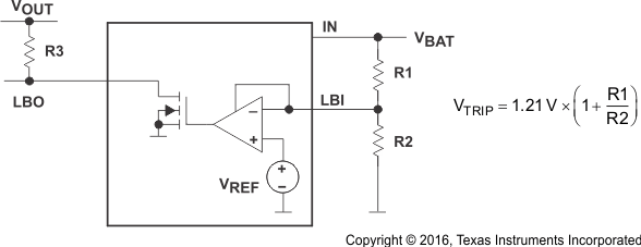
The internal low battery comparator trips at 1.21 V ±5% when the voltage on pin LBI ramps down. The battery voltage at which the comparator initiates a low battery warning at the LBO output can easily be programmed with a resistive divider as shown in Figure 34. TI recommends the sum of resistors R1 and R2 be in the range of
100 kΩ to 1 MΩ.
LBO is an open drain output. TI recommends an external pullup resistor to OUT in the 100-kΩ to 1-MΩ range. During start-up, the LBO output signal is invalid for the first 500 µs. LBO is high impedance when the device is disabled.
If the low battery comparator function is not used, connect LBI to ground and leave LBO unconnected.
 Figure 21. Programming of the Low Battery Comparator Trip Voltage
Use Equation 1 and Equation 2 to calculate the resistive divider for low battery detection with VLBI = 1.15 V to 1.27 V.


Use Equation 3 and Equation 4 to calculate the minimum and maximum battery voltage that triggers the low battery detector.


Table 4 lists the recommended values for the resistive divider.
Table 4. Recommended Values for the Resistive Divider From the E96 Series (±1%),
VLBI = 1.15 V to 1.27 V
| VBAT/V | R1/kΩ | R2/kΩ | VBAT(MIN)/V | VBAT(MAX)/V | ||
|---|---|---|---|---|---|---|
| 2.7 | 562 | 453 | 2.548 | −5.61% | 2.877 | 6.57% |
| 2.8 | 576 | 442 | 2.619 | −6.47% | 2.958 | 5.66% |
| 2.9 | 590 | 422 | 2.726 | −6% | 3.081 | 6.26% |
| 3 | 590 | 402 | 2.804 | −6.53% | 3.172 | 5.72% |
| 3.1 | 604 | 383 | 2.928 | −5.56% | 3.313 | 6.88% |
| 3.2 | 619 | 374 | 3.016 | −5.76% | 3.414 | 6.7% |
| 3.3 | 649 | 374 | 3.106 | −5.88% | 3.518 | 6.62% |
A 100-nF bypass capacitor must be connected in parallel to R2 if large line transients are expected. These voltage drops can inadvertently trigger the low battery comparator and produce a wrong low battery warning signal at the LBO pin.
9.3.8 Power Good Detector (TPS60131 and TPS60133)
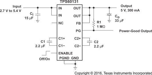
The PG pin is an open-drain output that is pulled low when the output is out of regulation. When the output voltage rises to about 90% of its nominal voltage, Power Good output is released. PG is high impedance when the device is disabled. An external pullup resistor must be connected between PG and OUT. The pullup resistor must be in the 100-kΩ to 1-MΩ range. If the Power Good function is not used, the PG-pin must remain unconnected.
 Figure 22. Typical Operating Circuit Using Power Good Comparator