SLVS258B November 1999 – December 2016 TPS60130 , TPS60131 , TPS60132 , TPS60133
PRODUCTION DATA.
- 1 Features
- 2 Applications
- 3 Description
- 4 Revision History
- 5 Device Options
- 6 Pin Configuration and Functions
- 7 Specifications
- 8 Parameter Measurement Information
- 9 Detailed Description
- 10Application and Implementation
- 11Power Supply Recommendations
- 12Layout
- 13Device and Documentation Support
- 14Mechanical, Packaging, and Orderable Information
Package Options
Mechanical Data (Package|Pins)
- PWP|20
Thermal pad, mechanical data (Package|Pins)
- PWP|20
Orderable Information
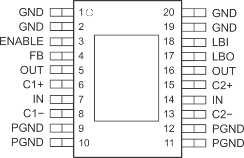
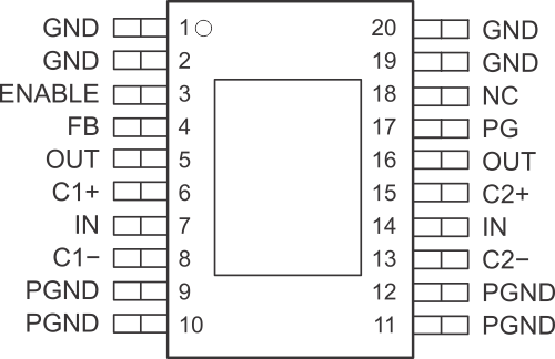
6 Pin Configuration and Functions
TPS60130 and TPS60132 PWP Package
20-Pin HTSSOP
Top View

TPS60131 and TPS60133 PWP Package
20-Pin HTSSOP
Top View

Pin Functions
| PIN | I/O | DESCRIPTION | |
|---|---|---|---|
| NAME | NO. | ||
| C1+ | 6 | — | Positive pin of the flying capacitor C1 |
| C1– | 8 | — | Negative pin of the flying capacitor C1 |
| C2+ | 15 | — | Positive pin of the flying capacitor C2 |
| C2– | 13 | — | Negative pin of the flying capacitor C2 |
| ENABLE | 3 | I | Enable input. Connect ENABLE to IN for normal operation. When ENABLE is a logic low, the device turns off and the supply current decreases to 0.05 µA. The output is disconnected from the input when the device is disabled. |
| FB | 4 | I | Feedback input. Connect FB to OUT as close to the load as possible to achieve best regulation. A resistive divider is on the chip to match internal reference voltage of 1.21 V. |
| GND | 1, 2, 19, 20 | — | Ground. Analog ground for internal reference and control circuitry. Connect to PGND pins through a short trace. |
| IN | 7, 14 | I | Supply input. Bypass IN to PGND with a capacitor that has half of the capacitance of the output capacitor. Connect both IN pins together through a short trace. |
| LBO/PG | 17 | O | Low battery detector output (TPS60130 and TPS60132) or Power Good output (TPS60131 and TPS60133). Open drain output of the low battery or Power Good comparator. It can sink 1 mA. TI recommends a 100-kΩ to 1-MΩ pullup resistor to OUT. Leave the pin unconnected if the low battery or Power Good detector is not used. |
| LBI/NC | 18 | I | Low battery detector input (TPS60130 and TPS60132 only). The voltage at this input is compared to the internal 1.21-V reference voltage. Connect this pin to ground if the low battery detection function is not used. On the TPS60131 and TPS60133, this pin is not connected. |
| OUT | 5, 16 | O | Regulated 5-V power output. Connect both OUT pins through a short trace and bypass OUT to GND with the output filter capacitor CO. |
| PGND | 9, 10, 11, 12 | — | Power ground. Charge-pump current flows through this pin. Connect all PGND pins together. |