SLVSA02B September 2009 – January 2019 TPS60151
PRODUCTION DATA.
- 1 Features
- 2 Applications
- 3 Description
- 4 Revision History
- 5 Device Comparison Table
- 6 Pin Configuration and Functions
- 7 Specifications
- 8 Detailed Description
- 9 Application and Implementation
- 10Power Supply Recommendations
- 11Layout
- 12Device and Documentation Support
- 13Mechanical, Packaging, and Orderable Information
Package Options
Mechanical Data (Package|Pins)
- DRV|6
Thermal pad, mechanical data (Package|Pins)
- DRV|6
Orderable Information
9.2.3 Application Curves
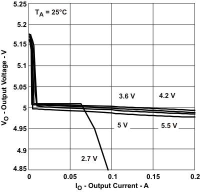 Figure 12. Output Voltage vs Output Current
 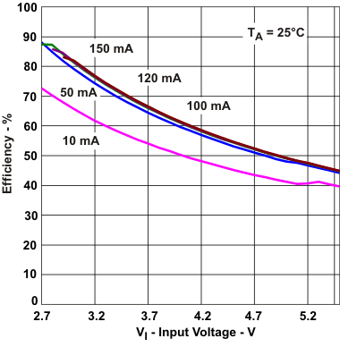 Figure 14. Efficiency vs Input Voltage
 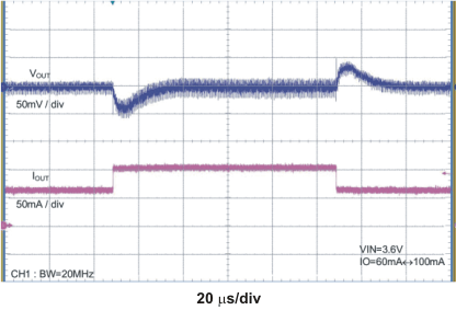 Figure 16. Load Transient Response
VIN = 3.6 V, Io = 60 mA to 100 mA
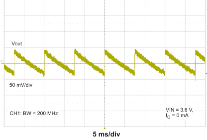 Figure 18. Load Transient
VCC = 3.6 V, Io = 0 mA
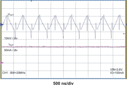 Figure 20. Output Ripple (Normal Mode)
VIN = 3.6 V, Io = 100 mA
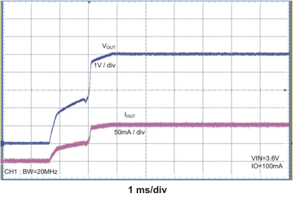 Figure 22. Power On
VIN = 3.6 V, Io = 100 mA
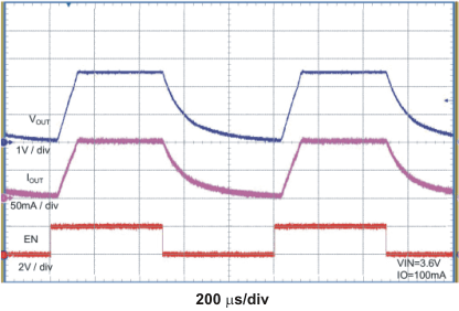 Figure 24. Enable / Disable
VIN = 3.6 V, Io = 100 mA
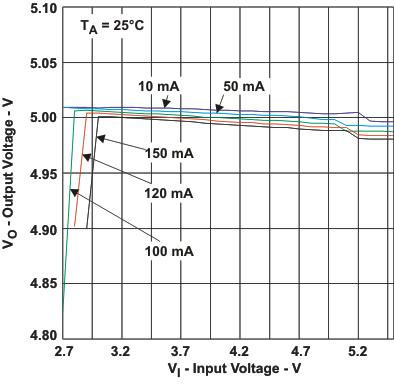 Figure 13. Output Voltage vs Input Voltage
 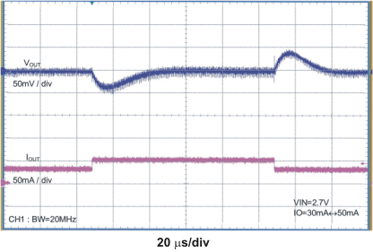 Figure 15. Load Transient Response
VIN = 2.7 V, Io = 30 mA to 50 mA
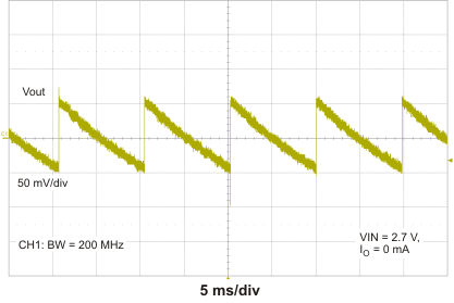 Figure 17. Output Ripple
VCC = 2.7 V, Io = 0 mA
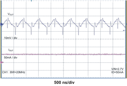 Figure 19. Output Ripple Voltage (Normal Mode)
VIN = 2.7 V, Io = 50 mA
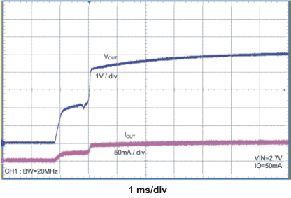 Figure 21. Power On
VIN = 2.7 V, Io = 50 mA
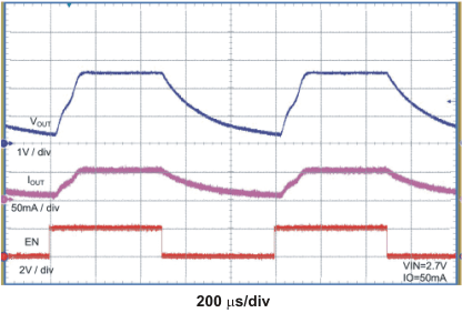 Figure 23. Enable / Disable
VIN = 2.7 V, Io = 50 mA
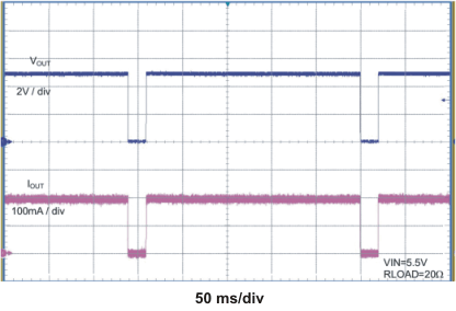 Figure 25. Thermal Shutdown Operation
VIN = 5.5 V, RLOAD= 20 Ω