SLVS324C July 2001 – October 2020 TPS60400 , TPS60401 , TPS60402 , TPS60403
PRODUCTION DATA
- 1 Features
- 2 Applications
- 3 Description
- 4 Revision History
- 5 Device Comparison Table
- 6 Pin Configuration and Functions
- 7 Specifications
- 8 Detailed Description
- 9 Application and Implementation
- 10Power Supply Recommendations
- 11Layout
- 12Device and Documentation Support
- 13Mechanical, Packaging, and Orderable Information
Package Options
Refer to the PDF data sheet for device specific package drawings
Mechanical Data (Package|Pins)
- DBV|5
Thermal pad, mechanical data (Package|Pins)
Orderable Information
9.3 System Examples
To reduce the output voltage ripple, a RC post filter can be used.
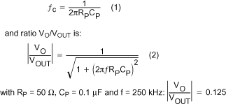
An output filter can easily be formed with a resistor (RP) and a capacitor (CP). Cutoff frequency is given by:
 Figure 9-4 TPS60400 with RC-Post Filter
The equation refers only to the relation between output and input of the ac ripple voltages of the filter.
To reduce the output voltage ripple, a LC post filter can be used.
Figure 9-5 shows a configuration with a LC-post filter to further reduce output ripple and noise.
 Figure 9-5 LC-Post Filter
The application allows to generate a voltage rail at a level of 1/2 of the input voltage.
A switched-capacitor voltage inverter can be configured as a high efficiency rail-splitter. This circuit provides a bipolar power supply that is useful in battery powered systems to supply dual-rail ICs, like operational amplifiers. Moreover, the SOT23-5 package and associated components require very little board space.
After power is applied, the flying capacitor (C(fly)) connects alternately across the output capacitors C3 and CO. This equalizes the voltage on those capacitors and draws current from VI to VO as required to maintain the output at 1/2 VI.
The maximum input voltage between VI and GND in the schematic (or between IN and OUT at the device itself) must not exceed 6.5 V.
 Figure 9-6 TPS60400 as a High-Efficiency Rail Splitter
The application allows to generate a voltage rail at a level of -Vi as well as 2 x Vi (V(pos)).
In the circuit of Figure 9-7, capacitors CI, C(fly), and CO form the inverter, while C1 and C2 form the doubler. C1 and C(fly) are the flying capacitors; CO and C2 are the output capacitors. Because both the inverter and doubler use part of the charge-pump circuit, loading either output causes both outputs to decline toward GND. Make sure the sum of the currents drawn from the two outputs does not exceed 60 mA. The maximum output current at V(pos) must not exceed 30 mA. If the negative output is loaded, this current must be further reduced.
 Figure 9-7 TPS60400 as Doubler/Inverter
The application generate a voltage rail at a level -2 x Vi.
Two devices can be cascaded to produce an even larger negative voltage (see Figure 9-8). The unloaded output voltage is normally -2 × VI, but this is reduced slightly by the output resistance of the first device multiplied by the quiescent current of the second. When cascading more than two devices, the output resistance rises dramatically.
 Figure 9-8 Doubling Inverter
The application allows to increase the output current by using two or more in parallel.
Paralleling multiple TPS6040xs reduces the output resistance. Each device requires its own flying capacitor (C(fly)), but the output capacitor (CO) serves all devices (see Figure 9-9). Increase CO's value by a factor of n, where n is the number of parallel devices. Equation 1 shows the equation for calculating output resistance.
 Figure 9-9 Paralleling Devices
The application adds a shutdown function.
If shutdown is necessary, use the circuit in Figure 9-10. The output resistance of the TPS6040x typically is 15 Ω plus two times the output resistance of the buffer.
Connecting multiple buffers in parallel reduces the output resistance of the buffer driving the IN pin.
 Figure 9-10 Shutdown Control
The application generates a regulated output voltage for a GaAs bias supply.
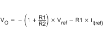
A solution for a -2.7-V/3-mA GaAs bias supply is proposed in Figure 9-11. The input voltage of 3.3 V is first inverted with a TPS60403 and stabilized using a TLV431 low-voltage shunt regulator. Resistor RP with capacitor CP is used for filtering the output voltage.
 Figure 9-11 GaAs Supply
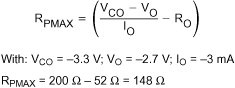
A 0.1-µF capacitor was selected for C(fly). By this, the output resistance of the inverter is about 52 Ω.
RPMAX can be calculated using the following equation:
A 100-Ω resistor was selected for RP.
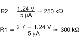
The reference voltage across R2 is 1.24 V typical. With 5-µA current for the voltage divider, R2 gets:
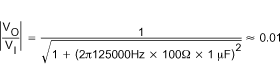
With CP = 1 µF the ratio VO/VI of the RC post filter is:
The application generates an output voltage of 1/2 of the input voltage.
By exchanging GND with OUT (connecting the GND pin with OUT and the OUT pin with GND), a step-down charge pump can easily be formed. In the first cycle S1 and S3 are closed, and C(fly) with CO in series are charged. Assuming the same capacitance, the voltage across C(fly) and CO is split equally between the capacitors. In the second cycle, S2 and S4 close and both capacitors with VI/2 across are connected in parallel.
The maximum input voltage between VI and GND in the schematic (or between IN and OUT at the device itself) must not exceed 6.5 V. For input voltages in the range of 6.5 V to 11 V, an additional Zener-diode is recommended (see Figure 9-14).
 Figure 9-12 Step-Down Principle
 Figure 9-13 Step-Down Charge Pump Connection
 Figure 9-14 Step-Down Charge Pump Connection for Higher Input Voltages