SLVS279D March 2000 – August 2015 TPS61000 , TPS61002 , TPS61005 , TPS61006 , TPS61007
PRODUCTION DATA.
- 1 Features
- 2 Applications
- 3 Description
- 4 Revision History
- 5 Available Options
- 6 Pin Configuration and Functions
- 7 Specifications
- 8 Parameter Measurement Information
- 9 Detailed Description
- 10Application and Implementation
- 11Power Supply Recommendations
- 12Layout
- 13Device and Documentation Support
- 14Mechanical, Packaging, and Orderable Information
Package Options
Refer to the PDF data sheet for device specific package drawings
Mechanical Data (Package|Pins)
- DGS|10
Thermal pad, mechanical data (Package|Pins)
Orderable Information
10 Application and Implementation
NOTE
Information in the following applications sections is not part of the TI component specification, and TI does not warrant its accuracy or completeness. TI’s customers are responsible for determining suitability of components for their purposes. Customers should validate and test their design implementation to confirm system functionality.
10.1 Application Information
The TPS6100x boost converter family is intended for systems that are powered by a single-cell NiCd or NiMH battery with a typical terminal voltage between 0.9 V to 1.6 V. It can also be used in systems that are powered by two-cell NiCd or NiMH batteries with a typical stack voltage between 1.8 V and 3.2 V. Additionally, singleor dual-cell, primary and secondary alkaline battery cells can be the power source in systems where the TPS6100x is used.
10.1.1 Schematic of TPS6100x Evaluation Modules (TPS6100XEVM156)
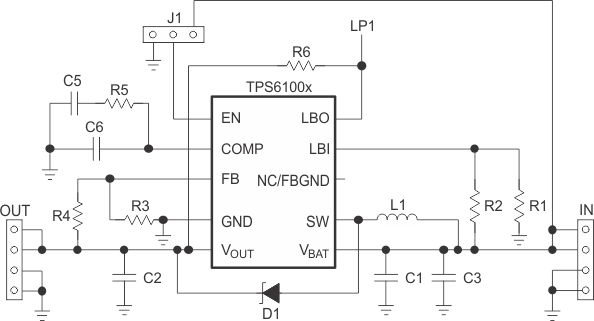 Figure 16. Schematic of TPS6100x Evaluation Modules
Evaluation modules are available for device types TPS61000, TPS61002, TPS61003, and TPS61006.
10.2 Typical Application
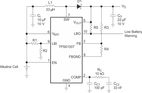 Figure 17. Typical Application Circuit for Adjustable Output Voltage Option
10.2.1 Design Requirements
See Table 2 for design parameters.
Table 2. TPS6100x Output Design Parameters
| DESIGN PARAMETERS | VALUES |
|---|---|
| Input voltage range | 1.8 V to 3.3 V |
| Output voltage | 3.3 V |
| Output voltage ripple | ±3% VOUT |
10.2.2 Detailed Design Procedure
10.2.2.1 Programming the TPS61000 and TPS61007 Adjustable Output Voltage Devices
The output voltage of the TPS61000 and TPS61007 can be adjusted with an external resistor divider. The typical value of the voltage on the FB pin is 500 mV in fixed-frequency operation and 485 mV in the power-save operation mode. The maximum allowed value for the output voltage is 3.3 V. The current through the resistive divider should be about 100 times greater than the current into the FB pin. The typical current into the FB pin is 0.01 µA, and the voltage across R4 is typically 500 mV. Based on those two values, the recommended value for R4 is in the range of 500 kΩ in order to set the divider current at 1 µA. From that, the value of resistor R3, depending on the needed output voltage VOUT, can be calculated using the following equation:

If, as an example, an output voltage of 2.5 V is needed, a 2-MΩ resistor should be chosen for R3.
The TPS61007 is an improved version of the TPS61000 adjustable output voltage device. The FBGND pin is internally connected to GND.
10.2.2.2 Programming the Low Battery Comparator Threshold Voltage
The current through the resistive divider should be about 100 times greater than the current into the LBI pin. The typical current into the LBI pin is 0.01 µA. The voltage across R2 is equal to the reference voltage that is generated on-chip, which has a value of 500 mV ±15 mV. The recommended value for R2 is therefore in the range of 500 kΩ. From that, the value of resistor R1, depending on the desired minimum battery voltage (VBAT), can be calculated using the following equation:

For example, if the low-battery detection circuit should flag an error condition on the LBO output pin at a battery voltage of 1 V, a resistor in the range of 500 kΩ should be chosen for R1.
The output of the low battery comparator is a simple open-drain output that goes active low if the battery voltage drops below the programmed threshold voltage on LBI. The output requires a pullup resistor with a recommended value of 1MΩ, and should only be pulled up to the VOUT. If not used, the LBO pin can be left floating.
10.2.2.3 Inductor Selection
The output filter of inductive switching regulators is a low pass filter of second order. It consists of an inductor and a capacitor, often referred to as storage inductor and output capacitor.
To select an inductor, keep the possible peak inductor current below the current limit threshold of the power switch in your chosen configuration. For example, the current limit threshold of the TPS61006’s switch is 1100 mA at an output voltage of 3.3 V. The highest peak current through the inductor and the switch depends on the output load, the input (VBAT), and the output voltage (VOUT). Estimation of the maximum average inductor current can be done using the following equation:

For example, for an output current of 100 mA at 3.3 V, at least 515-mA current flows through the inductor at a minimum input voltage of 0.8 V.
The second parameter for choosing the inductor is the desired current ripple in the inductor. Normally it is advisable to work with a ripple of less than 20% of the average inductor current. A smaller ripple reduces the magnetic hysteresis losses in the inductor as well as output voltage ripple and EMI. But in the same way, the regulation time at load change rises. In addition, a larger inductor increases the total system cost.
With those parameters it is possible to calculate the value for the inductor:

where
- f is the switching frequency
- ΔIL is the ripple current in the inductor, that is 20% x IL
In this example, the desired inductor has the value of 12 µH. With this calculated value and the calculated currents, it is possible to chose a suitable inductor. Care has to be taken that load transients and losses in the circuit can lead to higher currents as estimated in equation 3. Also, the losses in the inductor caused by magnetic hysteresis losses and copper losses are a major parameter for total circuit efficiency.
The following inductors from different suppliers were tested. All work with the TPS6100x converter within their specified parameters:
Table 3. Recommended Inductors
| VENDOR | PART NUMBER |
|---|---|
| Coilcraft | DO1608P Series |
| DS1608P Series | |
| DO3308 Series | |
| Coiltronics | UP1B Series |
| UP2B Series | |
| Murata | LQH3N Series |
| Sumida | CD43 Series |
| CD54 Series | |
| CDR74B Series | |
| TDK | NLC453232T Series |
10.2.2.4 Capacitor Selection
The major parameter necessary to define the output capacitor is the maximum allowed output voltage ripple of the converter. This ripple is determined by two parameters of the capacitor, the capacitance and the ESR. It is possible to calculate the minimum capacitance needed for the defined ripple, supposing that the ESR is zero.

where
- f is the switching frequency
- ΔV is the maximum allowed ripple.
With a chosen ripple voltage of 15 mV, a minimum capacitance of 10 µF is needed. The total ripple will be larger due to the ESR of the output capacitor. This additional component of the ripple can be calculated using the following equation:

An additional ripple of 30 mV is the result of using a tantalum capacitor with a low ESR of 300 mΩ. The total ripple is the sum of the ripple caused by the capacitance and the ripple caused by the ESR of the capacitor. In this example, the total ripple is 45 mV. It is possible to improve the design by enlarging the capacitor or using smaller capacitors in parallel to reduce the ESR or by using better capacitors with lower ESR, like ceramics. For example, a 10-µF ceramic capacitor with an ESR of 50 mΩ is used on the evaluation module (EVM). Tradeoffs have to be made between performance and costs of the converter circuit.
A 10-µF input capacitor is recommended to improve transient behavior of the regulator. A ceramic capacitor or a tantalum capacitor with a 100-nF ceramic capacitor in parallel placed close to the IC is recommended.
10.2.2.5 Rectifier Selection
The rectifier diode has a major impact on the overall converter efficiency. Standard diodes are not suitable for low-voltage switched mode power supplies. A Schottky diode with low forward voltage and fast reverse recovery should be used as a rectifier to minimize overall losses of the dc-dc converter. The maximum current rating of the diode must be high enough for the application. The maximum diode current is equal to the maximum current in the inductor that was calculated in equation 3. The maximum reverse voltage is the output voltage. The chosen diode should therefore have a reverse voltage rating higher than the output voltage.
Table 4. Recommended Diodes
| VENDOR | PART NUMBER |
|---|---|
| Motorola Surface Mount | MBRM120LT3 |
| MBR0520LT1 | |
| Motorola Axial Lead | 1N1517 |
| RB520S-30 | |
| ROHM | RB160L–40 |
The typical forward voltage of those diodes is in the range of 0.35 to 0.45 V assuming a peak diode current of 600 mA.
10.2.2.6 Compensation of the Control Loop
An R/C/C network must be connected to the COMP pin in order to stabilize the control loop of the converter. Both the pole generated by the inductor L1 and the zero caused by the ESR and capacitance of the output capacitor must be compensated. The network shown in Figure 18 satisfies these requirements.
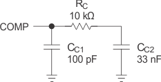 Figure 18. Compensation of the Control Loop
Resistor RC and capacitor CC2 depend on the chosen inductance. For a 33-µH inductor, the capacitance of CC2 should be chosen to 33 nF, or in other words, if the inductor is xx µH, the chosen compensation capacitor should be xx nF, the same number value. The value of the compensation resistor is then chosen based on the requirement to have a time constant of 0.3 ms for the R/C network of RC and CC2; hence for a 33-nF capacitor, a 10-kΩ resistor should be chosen for RC.
Capacitor CC1 is depending on the ESR and capacitance value of the output capacitor, and on the value chosen for RC. Its value is calculated using following equation:

For a selected output capacitor of 22 µF with an ESR of 0.2 Ω, and RC of 33 kΩ, the value of CC1 is in the range of 100 pF.
Table 5. Recommended Compensation Components
| INDUCTOR [µH] |
OUTPUT CAPACITOR | RC
[kΩ] |
CC1
[pF] |
CC2
[nF] |
|
|---|---|---|---|---|---|
| CAPACITANCE [µF] |
ESR [Ω] |
||||
| 33 | 22 | 0.2 | 10 | 100 | 33 |
| 22 | 22 | 0.3 | 15 | 100 | 22 |
| 10 | 22 | 0.4 | 33 | 100 | 10 |
| 10 | 10 | 0.1 | 33 | 100 | 10 |
10.2.3 Application Curves
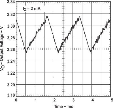 Figure 19. TPS61006 Output Voltage Ripple Amplitude
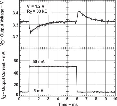 Figure 21. TPS61006 Load Transient Response
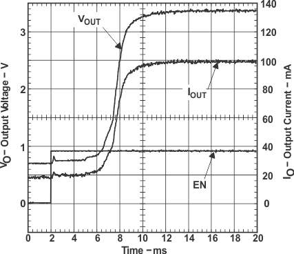 Figure 23. TPS61006 Start-up Timing Into 33-Ω Load
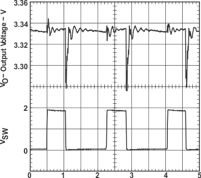 Figure 20. TPS61006 Output Voltage Ripple Amplitude
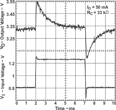 Figure 22. TPS61006 Line Transient Response