SLVSF14B September 2019 – August 2020 TPS61023
PRODUCTION DATA
- 1 Features
- 2 Applications
- 3 Description
- 4 Revision History
- 5 Pin Configuration and Functions
- 6 Specifications
- 7 Detailed Description
- 8 Application and Implementation
- 9 Power Supply Recommendations
- 10Layout
- 11Device and Documentation Support
- 12Mechanical, Packaging, and Orderable Information
Package Options
Mechanical Data (Package|Pins)
- DRL|6
Thermal pad, mechanical data (Package|Pins)
3 Description
TPS61023 device is a synchronous boost converter with 0.5-V ultra-low input voltage. The device provides a power supply solution for portable equipment and smart devices powered by various batteries and super capacitors. The TPS61023 has typical 3.7-A valley switch current limit over full temperature range. With a wide input voltage range of 0.5 V to 5.5 V, the TPS61023 supports super capacitor backup power applications, which may deeply discharge the super capacitor.
The TPS61023 operates at 1-MHz switching frequency when the input voltage is above 1.5 V. The switching frequency decreases gradually to 0.5 MHz when the input voltage is below 1.5 V down to 1 V. The TPS61023 enters power-save mode at light load condition to maintain high efficiency over the entire load current range. The TPS61023 consumes a 20-µA quiescent current from VOUT in light load condition. During shutdown, the TPS61023 is completely disconnected from the input power and only consumes a 0.1-µA current to achieve long battery life. The TPS61023 has 5.7-V output overvoltage protection, output short circuit protection, and thermal shutdown protection.
The TPS61023 offers a very small solution size with 1.2-mm × 1.6-mm SOT563 (DRL) package and minimum amount of external components.
| PART NUMBER | PACKAGE(1) | BODY SIZE (NOM) |
|---|---|---|
| TPS61023 | SOT563 (6) | 1.20 mm × 1.60 mm |
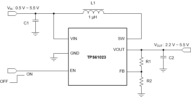
 Typical Application Circuit