SLVSGI6D october 2022 – september 2023 TPS61033 , TPS610333
PRODUCTION DATA
- 1
- 1 Features
- 2 Applications
- 3 Description
- 4 Device Comparison Table
- 5 Revision History
- 6 Pin Configuration and Functions
- 7 Specifications
-
8 Detailed Description
- 8.1 Overview
- 8.2 Functional Block Diagram
- 8.3
Feature Description
- 8.3.1 Undervoltage Lockout
- 8.3.2 Enable and Soft Start
- 8.3.3 Setting the Output Voltage
- 8.3.4 Current Limit Operation
- 8.3.5 Pass-Through Operation
- 8.3.6 Power Good Indicator
- 8.3.7 Implement Output Discharge by PG function
- 8.3.8 Overvoltage Protection
- 8.3.9 Output Short-to-Ground Protection
- 8.3.10 Thermal Shutdown
- 8.4 Device Functional Modes
- 9 Application and Implementation
- 10Device and Documentation Support
- 11Mechanical, Packaging, and Orderable Information
Package Options
Mechanical Data (Package|Pins)
- DRL|8
Thermal pad, mechanical data (Package|Pins)
Orderable Information
8.3.3 Setting the Output Voltage
There are two ways to set the output voltage of the TPS61033: adjustable or fixed. If the FB is connected to VIN, the TPS61033 works as a fixed 5.0-V output voltage version, the TPS61033 uses the internal resistor divider.
The output voltage is also can be set by an external resistor divider (R1, R2 in Figure 9-1). When the output voltage is regulated, the typical voltage at the FB pin is VREF. Thus the resistor divider is determined by Equation 5.
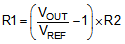
where
- VOUT is the regulated output voltage
- VREF is the internal reference voltage at the FB pin
TPS610333 can only support fixed 5.0-V output voltage, so FB should be connected with VIN rather than external resistor divider.