SLVSGI6D october 2022 – september 2023 TPS61033 , TPS610333
PRODUCTION DATA
- 1
- 1 Features
- 2 Applications
- 3 Description
- 4 Device Comparison Table
- 5 Revision History
- 6 Pin Configuration and Functions
- 7 Specifications
-
8 Detailed Description
- 8.1 Overview
- 8.2 Functional Block Diagram
- 8.3
Feature Description
- 8.3.1 Undervoltage Lockout
- 8.3.2 Enable and Soft Start
- 8.3.3 Setting the Output Voltage
- 8.3.4 Current Limit Operation
- 8.3.5 Pass-Through Operation
- 8.3.6 Power Good Indicator
- 8.3.7 Implement Output Discharge by PG function
- 8.3.8 Overvoltage Protection
- 8.3.9 Output Short-to-Ground Protection
- 8.3.10 Thermal Shutdown
- 8.4 Device Functional Modes
- 9 Application and Implementation
- 10Device and Documentation Support
- 11Mechanical, Packaging, and Orderable Information
Package Options
Mechanical Data (Package|Pins)
- DRL|8
Thermal pad, mechanical data (Package|Pins)
Orderable Information
8.3.4 Current Limit Operation
The TPS61033 uses a valley current limit sensing scheme. Current limit detection occurs during the off-time by sensing of the voltage drop across the synchronous rectifier.
When the load current is increased such that the inductor current is above the current limit within the whole switching cycle time, the off-time is increased to allow the inductor current to decrease to this threshold before the next on-time begins (so called frequency foldback mechanism). When the current limit is reached, the output voltage decreases during further load increase.
The maximum continuous output current (IOUT(LC)), before entering current limit (CL) operation, can be defined by Equation 2.
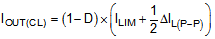
where
- D is the duty cycle
- ΔIL(P-P) is the inductor ripple current
The duty cycle can be estimated by Equation 3.

where
- VOUT is the output voltage of the boost converter
- VIN is the input voltage of the boost converter
- η is the efficiency of the converter, use 90% for most applications
The peak-to-peak inductor ripple current is calculated by Equation 4.
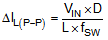
where
- L is the inductance value of the inductor
- fSW is the switching frequency
- D is the duty cycle
- VIN is the input voltage of the boost converter