SLVSH62 November 2023 TPS61033-Q1 , TPS610333-Q1
PRODUCTION DATA
- 1
- 1 Features
- 2 Applications
- 3 Description
- 4 Device Comparison Table
- 5 Pin Configuration and Functions
- 6 Specifications
-
7 Detailed Description
- 7.1 Overview
- 7.2 Functional Block Diagram
- 7.3
Feature Description
- 7.3.1 Undervoltage Lockout
- 7.3.2 Enable and Soft Start
- 7.3.3 Setting the Output Voltage
- 7.3.4 Current Limit Operation
- 7.3.5 Pass-Through Operation
- 7.3.6 Power Good Indicator
- 7.3.7 Implement Output Discharge by PG function
- 7.3.8 Spread Spectrum Frequency Modulation
- 7.3.9 Overvoltage Protection
- 7.3.10 Output Short-to-Ground Protection
- 7.3.11 Thermal Shutdown
- 7.4 Device Functional Modes
- 8 Application and Implementation
- 9 Device and Documentation Support
- 10Revision History
- 11Mechanical, Packaging, and Orderable Information
Package Options
Mechanical Data (Package|Pins)
- DRL|8
Thermal pad, mechanical data (Package|Pins)
Orderable Information
8.2.2.3 Output Capacitor Selection
The output capacitor is mainly selected to meet the requirements for output ripple and loop stability. The ripple voltage is related to capacitor capacitance and its equivalent series resistance (ESR). Assuming a ceramic capacitor with zero ESR, the minimum capacitance needed for a given ripple voltage can be calculated by Equation 9.
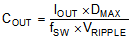
where
- DMAX is the maximum switching duty cycle
- VRIPPLE is the peak-to-peak output ripple voltage
- IOUT is the maximum output current
- fSW is the switching frequency
The ESR impact on the output ripple must be considered if tantalum or aluminum electrolytic capacitors are used. The output peak-to-peak ripple voltage caused by the ESR of the output capacitors can be calculated by Equation 10.

Take care when evaluating the derating of a ceramic capacitor under dc bias voltage, aging, and ac signal. For example, the dc bias voltage can significantly reduce capacitance. A ceramic capacitor can lose more than 50% of its capacitance at its rated voltage. Therefore, always leave margin on the voltage rating to ensure adequate capacitance at the required output voltage. Increasing the output capacitor makes the output ripple voltage smaller in PWM mode.
TI recommends using the X5R or X7R ceramic output capacitor in the range of 4-μF to 1000-μF effective capacitance, using 10-μF effective capacitance when output current is lower than 1 A and 20-μF when output current is higher than 1 A. The output capacitor affects the small signal control loop stability of the boost regulator. If the output capacitor is below the range, the boost regulator can potentially become unstable. Increasing the output capacitor makes the output ripple voltage smaller in PWM mode.