SGLS276D January 2005 – March 2016 TPS61040-Q1 , TPS61041-Q1
PRODUCTION DATA.
- 1 Features
- 2 Applications
- 3 Description
- 4 Revision History
- 5 Pin Configuration and Functions
- 6 Specifications
- 7 Detailed Description
- 8 Application and Implementation
- 9 Power Supply Recommendations
- 10Layout
- 11Device and Documentation Support
- 12Mechanical, Packaging, and Orderable Information
Package Options
Refer to the PDF data sheet for device specific package drawings
Mechanical Data (Package|Pins)
- DBV|5
Thermal pad, mechanical data (Package|Pins)
Orderable Information
1 Features
- Qualified for Automotive Applications
- 1.8-V to 6-V Input Voltage Range
- Adjustable Output Voltage Range Up to 28 V
- 400-mA (TPS61040-Q1) and 250-mA (TPS61041-Q1) Internal Switch Current
- Up to 1-MHz Switching Frequency
- 28-µA Typical No Load Quiescent Current
- 1-µA Typical Shutdown Current
- Internal Soft Start
- Space-Saving, 5-Pin SOT-23 Package
2 Applications
3 Description
The TPS6104x-Q1 devices are high-frequency boost converters for automotive applications. The devices are ideal for generating output voltages up to 28 V from a pre-regulated low voltage rail, dual-cell NiMH/NiCd or a single-cell Li-Ion battery, supporting input voltages from 1.8 V to 6 V.
The TPS6104x-Q1 devices operate with a switching frequency up to 1 MHz, allowing the use of small external components such as ceramic as well as tantalum output capacitors. Combined with the space-saving, 5-pin SOT-23 package, the TPS6104x-Q1 devices accomplish a small overall solution size. The TPS61040-Q1 device has an internal 400-mA switch current limit, while the TPS61041-Q1 device has a 250-mA switch current limit, offering lower output voltage ripple and allowing the use of a smaller form factor inductor for lower-power applications.
The TPS6104x-Q1 devices operate in a pulse frequency modulation (PFM) scheme with constant peak current control. The combination of low quiescent current (28 µA typical) and the optimized control scheme enable operation of the devices at high efficiencies over the entire load current range.
Device Information(1)
| PART NUMBER | PACKAGE | BODY SIZE (NOM) |
|---|---|---|
| TPS6104x-Q1 | SOT-23 (5) | 2.90 mm × 1.60 mm |
- For all available packages, see the orderable addendum at the end of the data sheet.
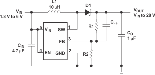
Typical Application Diagram

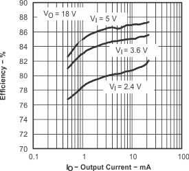
Efficiency vs Output Current
