SLVS465C December   2003  – February 2016 TPS61043

PRODUCTION DATA.  

  1. Features
  2. Applications
  3. Description
  4. Revision History
  5. Pin Configuration and Functions
  6. Specifications
    1. 6.1 Absolute Maximum Ratings
    2. 6.2 ESD Ratings
    3. 6.3 Recommended Operating Conditions
    4. 6.4 Thermal Information
    5. 6.5 Electrical Characteristics
    6. 6.6 Typical Characteristics
  7. Parameter Measurement Information
  8. Detailed Description
    1. 8.1 Overview
    2. 8.2 Functional Block Diagram
    3. 8.3 Feature Description
      1. 8.3.1 Operation
      2. 8.3.2 Boost Converter
      3. 8.3.3 Peak Current Control (Boost Converter)
      4. 8.3.4 Softstart
      5. 8.3.5 Control (CTRL)
    4. 8.4 Device Functional Modes
      1. 8.4.1 Overvoltage Protection (OVP)
      2. 8.4.2 Undervoltage Lockout
      3. 8.4.3 Thermal Shutdown
  9. Application and Implementation
    1. 9.1 Application Information
      1. 9.1.1 Efficiency
      2. 9.1.2 Setting the LED Current
      3. 9.1.3 Analog Control Signal for Brightness Control
      4. 9.1.4 PWM Control With Separate Enable
    2. 9.2 Typical Application
      1. 9.2.1 Design Requirements
      2. 9.2.2 Detailed Design Procedure
        1. 9.2.2.1 Inductor Selection, Maximum Load Current, and Switching Frequency
        2. 9.2.2.2 Output Capacitor Selection and Line Regulation
        3. 9.2.2.3 Input Capacitor Selection
        4. 9.2.2.4 Diode Selection
      3. 9.2.3 Application Curves
    3. 9.3 System Examples
      1. 9.3.1 TPS61043 With 1-mm Total System Height
      2. 9.3.2 TPS61043 With Low LED Ripple Current and Higher Accuracy Using a 4.7-µF Output Capacitor
      3. 9.3.3 TPS61043 Powering 3 LEDs
      4. 9.3.4 Adjustable Brightness Control Using an Analog Voltage
      5. 9.3.5 Alternative Adjustable Brightness Control Using PWM Signal
  10. 10Power Supply Recommendations
  11. 11Layout
    1. 11.1 Layout Guidelines
    2. 11.2 Layout Example
    3. 11.3 Thermal Considerations
  12. 12Device and Documentation Support
    1. 12.1 Device Support
      1. 12.1.1 Third-Party Products Disclaimer
    2. 12.2 Documentation Support
      1. 12.2.1 Related Documentation
    3. 12.3 Community Resources
    4. 12.4 Trademarks
    5. 12.5 Electrostatic Discharge Caution
    6. 12.6 Glossary
  13. 13Mechanical, Packaging, and Orderable Information

Package Options

Refer to the PDF data sheet for device specific package drawings

Mechanical Data (Package|Pins)
  • DRB|8
Thermal pad, mechanical data (Package|Pins)
Orderable Information

11 Layout

11.1 Layout Guidelines

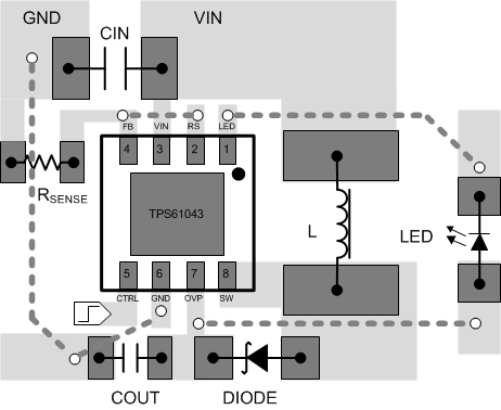
In all switching power supplies the layout is an important step in the design, especially at high peak currents and switching frequencies. If the layout is not carefully done, the regulator might show noise problems and duty cycle jitter.

The input capacitor should be placed as close as possible to the input pin for good input voltage filtering. The inductor and diode must be placed as close as possible to the switch pin to minimize noise coupling into other circuits. It is important to connect the output capacitor directly across the diode cathode pin and ground rather than connecting the output capacitor across the LEDs. This minimizes EMI. Because the feedback pin and network is a high-impedance circuit, the feedback network should be routed away from the inductor.

11.2 Layout Example

TPS61043 layoutexample2_SLVS465.gif Figure 25. Layout Example

11.3 Thermal Considerations

The TPS61043 comes in a thermally enhanced QFN package. The package includes a thermal pad improving the thermal capabilities of the package. See QFN/SON PCB Attachment (SLUA271).

The thermal resistance junction to ambient RΘJA of the QFN package greatly depends on the PCB layout. Using thermal vias and wide PCB traces improves the thermal resistance R ΘJA. Under normal operation conditions no PCB vias are required for the thermal pad. However, the thermal pad must be soldered to the PCB.