SLVS465C December   2003  – February 2016 TPS61043

PRODUCTION DATA.  

  1. Features
  2. Applications
  3. Description
  4. Revision History
  5. Pin Configuration and Functions
  6. Specifications
    1. 6.1 Absolute Maximum Ratings
    2. 6.2 ESD Ratings
    3. 6.3 Recommended Operating Conditions
    4. 6.4 Thermal Information
    5. 6.5 Electrical Characteristics
    6. 6.6 Typical Characteristics
  7. Parameter Measurement Information
  8. Detailed Description
    1. 8.1 Overview
    2. 8.2 Functional Block Diagram
    3. 8.3 Feature Description
      1. 8.3.1 Operation
      2. 8.3.2 Boost Converter
      3. 8.3.3 Peak Current Control (Boost Converter)
      4. 8.3.4 Softstart
      5. 8.3.5 Control (CTRL)
    4. 8.4 Device Functional Modes
      1. 8.4.1 Overvoltage Protection (OVP)
      2. 8.4.2 Undervoltage Lockout
      3. 8.4.3 Thermal Shutdown
  9. Application and Implementation
    1. 9.1 Application Information
      1. 9.1.1 Efficiency
      2. 9.1.2 Setting the LED Current
      3. 9.1.3 Analog Control Signal for Brightness Control
      4. 9.1.4 PWM Control With Separate Enable
    2. 9.2 Typical Application
      1. 9.2.1 Design Requirements
      2. 9.2.2 Detailed Design Procedure
        1. 9.2.2.1 Inductor Selection, Maximum Load Current, and Switching Frequency
        2. 9.2.2.2 Output Capacitor Selection and Line Regulation
        3. 9.2.2.3 Input Capacitor Selection
        4. 9.2.2.4 Diode Selection
      3. 9.2.3 Application Curves
    3. 9.3 System Examples
      1. 9.3.1 TPS61043 With 1-mm Total System Height
      2. 9.3.2 TPS61043 With Low LED Ripple Current and Higher Accuracy Using a 4.7-µF Output Capacitor
      3. 9.3.3 TPS61043 Powering 3 LEDs
      4. 9.3.4 Adjustable Brightness Control Using an Analog Voltage
      5. 9.3.5 Alternative Adjustable Brightness Control Using PWM Signal
  10. 10Power Supply Recommendations
  11. 11Layout
    1. 11.1 Layout Guidelines
    2. 11.2 Layout Example
    3. 11.3 Thermal Considerations
  12. 12Device and Documentation Support
    1. 12.1 Device Support
      1. 12.1.1 Third-Party Products Disclaimer
    2. 12.2 Documentation Support
      1. 12.2.1 Related Documentation
    3. 12.3 Community Resources
    4. 12.4 Trademarks
    5. 12.5 Electrostatic Discharge Caution
    6. 12.6 Glossary
  13. 13Mechanical, Packaging, and Orderable Information

Package Options

Refer to the PDF data sheet for device specific package drawings

Mechanical Data (Package|Pins)
  • DRB|8
Thermal pad, mechanical data (Package|Pins)
Orderable Information

5 Pin Configuration and Functions

DRB Package
8-PIN VSON
Top View
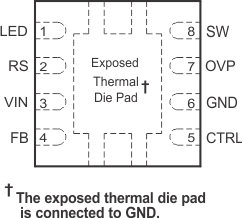
TPS61043 pin_out_lvs441.gif

Pin Functions

PIN I/O DESCRIPTION
NAME NO.
CTRL 5 I Combined enable and PWM control pin. If CTRL is constantly pulled high, the device is enabled and the internal LED switch (Q2) is constantly turned on. When CTRL is pulled to GND, the device is disabled. Apply a PWM signal (100 Hz to 50 kHz) to this pin to control the brightness of the LEDs
FB 4 I Feedback. FB regulates the LED current through the sense resistor by regulating the voltage across RS to
252 mV.
GND 6 GND
LED 1 I Input of the LED switch (Q2). Connect the LEDs to this pin.
OVP 7 I Overvoltage protection. OVP is connected to the output capacitor of the converter.
RS 2 O Output of the internal LED switch. The sense resistor that programs the LED current is connected to RS.
SW 8 I Drain of the integrated switch (Q1)
VIN 3 I Input supply pin.