SLVSAA5A May 2010 – December 2015 TPS61071-Q1
UNLESS OTHERWISE NOTED, this document contains PRODUCTION DATA.
- 1 Features
- 2 Applications
- 3 Description
- 4 Revision History
- 5 Pin Configuration and Functions
- 6 Specifications
- 7 Detailed Description
- 8 Application and Implementation
- 9 Power Supply Recommendations
- 10Layout
- 11Device and Documentation Support
- 12Mechanical, Packaging, and Orderable Information
Package Options
Mechanical Data (Package|Pins)
- DDC|6
Thermal pad, mechanical data (Package|Pins)
Orderable Information
8 Application and Implementation
NOTE
Information in the following applications sections is not part of the TI component specification, and TI does not warrant its accuracy or completeness. TI’s customers are responsible for determining suitability of components for their purposes. Customers should validate and test their design implementation to confirm system functionality.
8.1 Application Information
The TPS61071-Q1 DC-DC converter is intended for systems powered by a single-cell, up to triple-cell alkaline, NiCd, NiMH battery with a typical terminal voltage between 0.9 V and 5.5 V. The TPS61071-Q1 device can also be used in systems powered by one-cell Li-ion or Li-polymer with a typical voltage between 2.5 V and 4.2 V. Additionally, any other voltage source with a typical output voltage between 0.9 V and 5.5 V can power systems where the TPS61071-Q1 is used. Due to the nature of boost converters, the output voltage regulation is only maintained when the input voltage applied is lower than the programmed output voltage.
8.2 Typical Applications
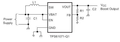 Figure 19. Typical Application Circuit
8.2.1 Design Requirements
In this example, TPS61071-Q1 is used to design a 3.3-V power supply with 75-mA output current capability supplied with an input voltage range from 0.9 V to 1.65 V.
8.2.2 Detailed Design Procedure
8.2.2.1 Programming the Output Voltage
The output voltage can be adjusted with an external resistor divider. The typical value of the voltage at the FB pin is 500 mV. The maximum recommended value for the output voltage is 5.5 V. The current through the resistive divider should be about 100 times greater than the current into the FB pin. The typical current into the FB pin is 0.01 µA, and the voltage across R2 is typically 500 mV. Based on those two values, the recommended value for R2 should be lower than 500 kΩ, in order to set the divider current at 1 µA or higher. Because of internal compensation circuitry, the value for this resistor should be in the range of 200 kΩ. From that, the value of resistor R1, depending on the needed output voltage (VO), is calculated using Equation 1:

For example, if an output voltage of 3.3 V is needed, a 1 MΩ resistor should be chosen for R1. If for any reason the value chosen for R2 is significantly lower than 200 kΩ, additional capacitance in parallel to R1 is recommended, if the device shows unstable regulation of the output voltage. The required capacitance value is calculated using Equation 2:

8.2.2.2 Inductor Selection L1
A boost converter normally requires two main passive components for storing energy during the conversion. A boost inductor and a storage capacitor at the output are required. To select the boost inductor, it is recommended to keep the possible peak inductor current below the current limit threshold of the power switch in the chosen configuration. For example, the current limit threshold of the TPS61071-Q1's switch is 600 mA. The highest peak current through the inductor and the switch depends on the output load, the input (VBAT), and the output voltage (VOUT). Estimation of the maximum average inductor current is done using Equation 3:

For example, for an output current of 75 mA at 3.3 V, at least 340 mA of average current flows through the inductor at a minimum input voltage of 0.9 V.
The second parameter for choosing the inductor is the desired current ripple in the inductor. Normally, it is advisable to work with a ripple of less than 20% of the average inductor current. A smaller ripple reduces the magnetic hysteresis losses in the inductor, as well as output voltage ripple and EMI. But in the same way, regulation time rises at load changes. In addition, a larger inductor increases the total system costs. With these parameters, it is possible to calculate the value for the inductor by using Equation 4:

Parameter f is the switching frequency and ΔIL is the ripple current in the inductor, i.e., 40% ΔIL. In this example, the desired inductor has the value of 4 µH. With this calculated value and the calculated currents, it is possible to choose a suitable inductor. In typical applications, a 4.7-µH inductance is recommended. The device has been optimized to operate with inductance values between 2.2 µH and 10 µH. Nevertheless, operation with higher inductance values may be possible in some applications. Detailed stability analysis is then recommended. Care must be taken because load transients and losses in the circuit can lead to higher currents as estimated in Equation 4. Also, the losses in the inductor caused by magnetic hysteresis losses and copper losses are a major parameter for total circuit efficiency.
Table 2 lists the inductor series from different suppliers which have been used with TPS6107x converters:
Table 2. List of Inductors
| VENDOR | INDUCTOR SERIES |
|---|---|
| TDK | VLF3010 |
| VLF4012 | |
| Wurth Elektronik | 744031xxx |
| 744042xxx | |
| EPCOS | B82462-G4 |
| Cooper Electronics Technologies | SD18 |
| SD20 | |
| Taiyo Yuden | CB2016B xxx |
| CB2518B xxx |
8.2.2.3 Capacitor Selection
8.2.2.3.1 Input Capacitor C1
TI recommends at least a 10-µF capacitor to improve transient behavior of the regulator and EMI behavior of the total power supply circuit. A ceramic capacitor or a tantalum capacitor with a 100-nF ceramic capacitor in parallel, placed close to the device, is recommended.
8.2.2.3.2 Output Capacitor C2
The major parameter necessary to define the output capacitor is the maximum allowed output voltage ripple of the converter. This ripple is determined by two parameters of the capacitor, the capacitance and the ESR. To calculate the minimum capacitance needed for the defined ripple, suppose that the ESR is zero and use Equation 5:

where
- Parameter f is the switching frequency and ΔV is the maximum allowed ripple.
With a chosen ripple voltage of 10 mV, a minimum capacitance of 4.5 µF is needed. In this value range, ceramic capacitors are a good choice. The ESR and the additional ripple created are negligible. It is calculated using Equation 6:

The total ripple is the sum of the ripple caused by the capacitance and the ripple caused by the ESR of the capacitor. Additional ripple is caused by load transients. This means that the output capacitor has to completely supply the load during the charging phase of the inductor. The value of the output capacitance depends on the speed of the load transients and the load current during the load change. With the calculated minimum value of 4.5 µF and load transient considerations, the recommended output capacitance value is in a 10 µF range.
Care must be taken on capacitance loss caused by derating due to the applied dc voltage and the frequency characteristic of the capacitor. For example, larger form factor capacitors (in 1206 size) have their self resonant frequencies in the same frequency range as the TPS61071-Q1 operating frequency. So the effective capacitance of the capacitors used may be significantly lower. Therefore, the recommendation is to use smaller capacitors in parallel instead of one larger capacitor.
8.2.2.4 Small Signal Stability
To analyze small signal stability in more detail, the small signal transfer function of the error amplifier and the regulator, which is given in Equation 7, can be used:

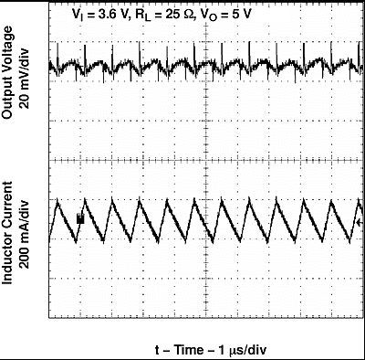
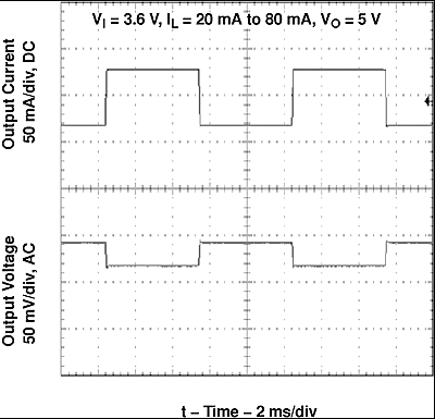
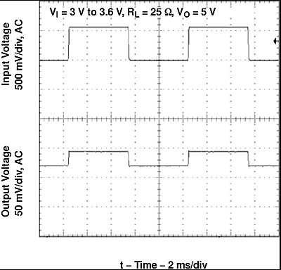
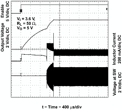
8.2.3 Application Curves
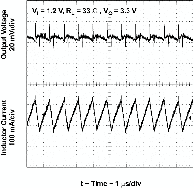
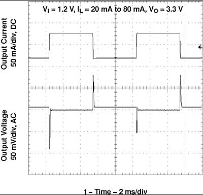
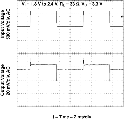
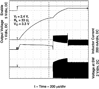
8.3 System Examples
 Figure 29. Power Supply Solution Having Small Total Solution Size
List of Components:
U1 = TPS61070DDC
L1 = 4.7 µH Taiyo Yuden CB2016B4R7M
c1 = 1 × 4.7 µF, 0603, X7R/X5R Ceramic
C2 = 2 × 4.7 µF, 0603, X7R/X5R Ceramic
 Figure 30. Power Supply Solution for Powering White LEDs in Lighting Applications
List of Components:
U1 = TPS61070DDC
L1 = 4.7 µH Taiyo Yuden CB2016B4R7M
c1 = 1 × 4.7 µF, 0603, X7R/X5R Ceramic
C2 = 2 × 4.7 µF, 0603, X7R/X5R Ceramic
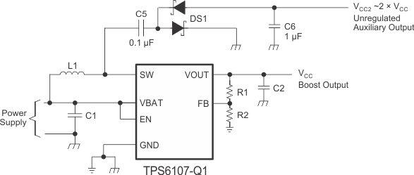 Figure 31. Power Supply Solution With Auxiliary Positive Output Voltage
List of Components:
U1 = TPS61070DDC
L1 = 4.7 µH Wurth Elektronik 744031004
c1 = 2 × 4.7 µF, 0603, X7R/X5R Ceramic
C2 = 2 × 4.7 µF, 0603, X7R/X5R Ceramic
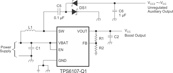 Figure 32. Power Supply Solution With Auxiliary Negative Output Voltage
List of Components:
U1 = TPS61070DDC
L1 = 4.7 µH Wurth Elektronik 744031004
c1 = 2 × 4.7 µF, 0603, X7R/X5R Ceramic
C2 = 2 × 4.7 µF, 0603, X7R/X5R Ceramic

