SLVSAA5A May   2010  – December 2015 TPS61071-Q1

UNLESS OTHERWISE NOTED, this document contains PRODUCTION DATA.  

  1. Features
  2. Applications
  3. Description
  4. Revision History
  5. Pin Configuration and Functions
  6. Specifications
    1. 6.1 Absolute Maximum Ratings
    2. 6.2 ESD Ratings
    3. 6.3 Recommended Operating Conditions
    4. 6.4 Thermal Information
    5. 6.5 Electrical Characteristics
    6. 6.6 Typical Characteristics
  7. Detailed Description
    1. 7.1 Overview
    2. 7.2 Functional Block Diagram
    3. 7.3 Feature Description
      1. 7.3.1 Controller Circuit
        1. 7.3.1.1 Synchronous Rectifier
        2. 7.3.1.2 Undervoltage Lockout
        3. 7.3.1.3 Soft Start and Short-Circuit Protection
    4. 7.4 Device Functional Modes
      1. 7.4.1 Device Enable
  8. Application and Implementation
    1. 8.1 Application Information
    2. 8.2 Typical Applications
      1. 8.2.1 Design Requirements
      2. 8.2.2 Detailed Design Procedure
        1. 8.2.2.1 Programming the Output Voltage
        2. 8.2.2.2 Inductor Selection L1
        3. 8.2.2.3 Capacitor Selection
          1. 8.2.2.3.1 Input Capacitor C1
          2. 8.2.2.3.2 Output Capacitor C2
        4. 8.2.2.4 Small Signal Stability
      3. 8.2.3 Application Curves
    3. 8.3 System Examples
  9. Power Supply Recommendations
  10. 10Layout
    1. 10.1 Layout Guidelines
    2. 10.2 Layout Example
    3. 10.3 Thermal Considerations
  11. 11Device and Documentation Support
    1. 11.1 Device Support
      1. 11.1.1 Third-Party Products Disclaimer
    2. 11.2 Community Resources
    3. 11.3 Trademarks
    4. 11.4 Electrostatic Discharge Caution
    5. 11.5 Glossary
  12. 12Mechanical, Packaging, and Orderable Information

Package Options

Mechanical Data (Package|Pins)
Thermal pad, mechanical data (Package|Pins)
Orderable Information

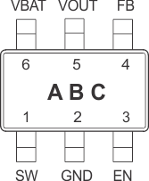
5 Pin Configuration and Functions

DDC Package
6-Pin SOT
Top View
TPS61071-Q1 po_lvs510.gif

Pin Functions

PIN I/O DESCRIPTION
NO. NAME
1 SW I Boost and rectifying switch input
2 GND Device (IC) ground connection for logic and power
3 EN I Enable input (1/VBAT enabled, 0/GND disabled)
4 FB I Voltage feedback for programming the output voltage
5 VOUT O Boost converter output
6 VBAT I Supply voltage