SLVSE09A April 2017 – April 2017 TPS61096A
PRODUCTION DATA.
- 1 Features
- 2 Applications
- 3 Description
- 4 Revision History
- 5 Pin Configuration and Functions
- 6 Specifications
- 7 Detailed Description
- 8 Application and Implementation
- 9 Power Supply Recommendations
- 10Layout
- 11Device and Documentation Support
- 12Mechanical, Packaging, and Orderable Information
Package Options
Mechanical Data (Package|Pins)
- DSS|12
Thermal pad, mechanical data (Package|Pins)
- DSS|12
Orderable Information
1 Features
- 1 µA ultra-low IQ into VIN pin
- Operating Input Voltage from 1.8 V to 5.5 V
- Adjustable Output Voltage from 4.5 V to 28 V
- Selectable Inductor Peak Current:
- 0.25 A and 0.5 A
- Integrated Power Diode
- Integrated Level Shifters
- 70% Efficiency at 10 µA load
- 12-Pin 3-mm x 2-mm WSON Package
- Create a Custom Design Using the TPS61096A With the WEBENCH® Power Designer
2 Applications
- Stylus
- Memory LCD Bias
- Sensor Power
- General Purpose Bias
- RF Mems Relay Power
3 Description
The TPS61096A is a high output voltage boost converter with ultra-low quiescent current. It is designed for products that require high efficiency at light load conditions powered by either two-cell alkaline, or one-cell Li-Ion or Li-polymer battery.
The TPS61096A integrates a 30-V power switch and a power diode. It can output up to 28 Volts. The TPS61096A uses a PFM peak current control scheme to obtain the highest efficiency over a wide range of input and output load conditions. It only consumes 1 µA quiescent current and can achieve up to 70% efficiency under 10-µA load condition.
The TPS61096A can also support selective inductor peak current. With 250-mA current limit, the TPS61096A can reduce inductor ripple so that it reduces external component size for light load applications. With 500 mA current limit, the TPS61096A can provide 30 mA output current for a conversion from 3.3 V to 18 V.
The TPS61096A integrates two-channel low-power level shifters to convert low level signals to output voltage level signals for specific applications. It only consumes 1-µA static current per channel and ensures very low static and dynamic power consumption across the entire output range.
The TPS61096A is available in a 12-pin 3.0-mm x 2.0-mm WSON Package.
Device Information(1)
| PART NUMBER | PACKAGE | BODY SIZE (NOM) |
|---|---|---|
| TPS61096A | WSON (12) | 3 mm x 2 mm |
- For all available packages, see the orderable addendum at the end of the data sheet.
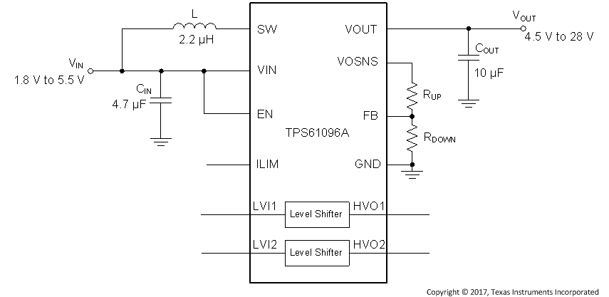
Typical Application Circuit
