SLVSE09A April 2017 – April 2017 TPS61096A
PRODUCTION DATA.
- 1 Features
- 2 Applications
- 3 Description
- 4 Revision History
- 5 Pin Configuration and Functions
- 6 Specifications
- 7 Detailed Description
- 8 Application and Implementation
- 9 Power Supply Recommendations
- 10Layout
- 11Device and Documentation Support
- 12Mechanical, Packaging, and Orderable Information
Package Options
Mechanical Data (Package|Pins)
- DSS|12
Thermal pad, mechanical data (Package|Pins)
- DSS|12
Orderable Information
6 Specifications
(1)| MIN | MAX | UNIT | |||
|---|---|---|---|---|---|
| Voltage range at terminals | VIN, EN, ILIM, LVI1, LVI2 | –0.3 | 6 | V | |
| FB | -0.3 | 3.6 | V | ||
| SW, VOUT, VOSNS, HVO1, HVO2 | –0.3 | 32 | V | ||
| Operating junction temperature, TJ | –40 | 150 | °C | ||
| Storage temperature, Tstg | –65 | 150 | °C | ||
(1) Stresses beyond those listed under Absolute Maximum Ratings may cause permanent damage to the device. These are stress ratings only, which do not imply functional operation of the device at these or any other conditions beyond those indicated under Recommended Operating Conditions. Exposure to absolute-maximum-rated conditions for extended periods may affect device reliability.
6.1 ESD Ratings
| VALUE | UNIT | |||
|---|---|---|---|---|
| V(ESD) | Electrostatic discharge | Human-body model (HBM), per ANSI/ESDA/JEDEC JS-001(1) | ± 2000 | V |
| Charged-device model (CDM), per JEDEC specification JESD22-C101(2) | ± 500 | |||
(1) JEDEC document JEP155 states that 500-V HBM allows safe manufacturing with a standard ESD control process. Manufacturing with less than 500-V HBM is possible with the necessary precautions.
(2) JEDEC document JEP157 states that 250-V CDM allows safe manufacturing with a standard ESD control process. Manufacturing with less than 250-V CDM is possible with the necessary precautions.
6.2 Recommended Operating Conditions
over operating free-air temperature range (unless otherwise noted)| MIN | NOM | MAX | UNIT | ||
|---|---|---|---|---|---|
| VIN | Input voltage | 1.8 | 5.5 | V | |
| VOUT | Boost converter output voltage | 4.5 | 28 | V | |
| L | Inductor | 1.0 | 2.2 | 47 | µH |
| CIN | Input capacitor | 1.0 | 4.7 | µF | |
| COUT | Output capacitor | 10 | 10 | 100 | µF |
| TJ | Operating junction temperature | –40 | 125 | °C | |
6.3 Thermal Information
| THERMAL METRIC(1) | TPS61096A | UNIT | |
|---|---|---|---|
| DSS (WSON) | |||
| 12 PINS | |||
| RθJA | Junction-to-ambient thermal resistance | 65.1 | °C/W |
| RθJC(top) | Junction-to-case (top) thermal resistance | 72.4 | °C/W |
| RθJB | Junction-to-board thermal resistance | 29.7 | °C/W |
| ψJT | Junction-to-top characterization parameter | 2.5 | °C/W |
| ψJB | Junction-to-board characterization parameter | 29.7 | °C/W |
| RθJC(bot) | Junction-to-case (bottom) thermal resistance | 10.7 | °C/W |
(1) For more information about traditional and new thermal metrics, see the Semiconductor and IC Package Thermal Metrics application report, SPRA953.
6.4 Electrical Characteristics
-40°C ≤ TJ ≤ 125°C and VIN=3.6V. Typical values are at TJ = 25°C, unless otherwise noted.| PARAMETER | TEST CONDITIONS | MIN | TYP | MAX | UNIT | |
|---|---|---|---|---|---|---|
| POWER SUPPLY | ||||||
| VIN | Input voltage range | 1.8 | 5.5 | V | ||
| VUVLO | Undervoltage lockout threshold | Input voltage rising | 1.5 | 1.7 | V | |
| Hysteresis | 0.2 | 0.3 | V | |||
| IQ_VIN | Quiescent current into VIN pin | Device enabled, no load, no switching -40°C ≤ TJ ≤ 85 °C |
1.2 | 2.5 | µA | |
| IQ_VOUT | Quiescent current into VOUT pin | Device enabled internal LS main switch on, VOSNS switch on VOUT = 20 V, IQ to level shifter excluded, -40°C ≤ TJ ≤ 85 °C |
0.2 | µA | ||
| ISD | Shutdown current into VIN pin | Device disabled -40°C ≤ TJ ≤ 85 °C |
0.07 | 0.3 | µA | |
| OUTPUT | ||||||
| VOUT | Output voltage range | 4.5 | 28 | V | ||
| VREF | Internal reference voltage | 0.98 | 1 | 1.02 | V | |
| IOUT_LKG | Leakage current into VOUT pin | Device disabled VOUT = 20 V -40°C ≤ TJ ≤ 85 °C |
0.2 | µA | ||
| IFB_LKG | Leakage current into FB pin | VFB = 1.0 V | 0.2 | µA | ||
| VOVP | Output overvoltage protection threshold | Rising edge at VOUT pin | 28.2 | 29.4 | 30.6 | V |
| VOVP_HYS | Overvoltage protection hysteresis | 0.4 | 0.8 | 1.2 | V | |
| POWER SWITCH AND CURRENT LIMIT | ||||||
| RDS(on) | MOSFET on-resistance | VIN = 3.6 V | 450 | 700 | mΩ | |
| IILIM | Peak switch current limit | ILIM = Low | 0.15 | 0.25 | 0.35 | A |
| ILIM = High | 0.35 | 0.5 | 0.6 | A | ||
| tSS | Soft-start time | 1 | 4.5 | ms | ||
| ISW_LKG | Leakage current into SW pin (from SW pin to GND) | Device disabled , VSW = 20 V -40°C ≤ TJ ≤ 85 °C |
0.5 | µA | ||
| LEVEL SHIFTER | ||||||
| IQ_LS | Level shifters quiescent current into VOUT pin | Both level shifter channel enabled, LVIx = Low | 0.5 | 1 | µA | |
| Both level shifter channel enabled, LVIx = High | 1.5 | 3 | µA | |||
| fPULSE | Pulse frequency | CHVOx ≤ 10 pF | 200 | kHz | ||
| VIL | Low level input voltage threshold at LVIx pin | Falling edge | 0.15 × Vin | V | ||
| VIH | High level input voltage threshold at LVIx pin | Rising edge | 0.8 × Vin | V | ||
| VOH | High-level output voltage at HVOx pin | 12 V ≤ VOUT ≤ 28 V IHVOx = 10 µA |
VOUT – 0.1 V | V | ||
| 12 V ≤ VOUT ≤ 28 V IHVOx = 100 µA |
VOUT – 0.3 V | V | ||||
| VOL | Low-level output voltage at HVOx | 12 V ≤ VOUT ≤ 28 V IHVOx = -10 µA |
0.1 | V | ||
| 12 V ≤ VOUT ≤ 28 V IHVOx = -100 µA |
0.3 | V | ||||
| ISRC | Level shifter high-side FET sourcing current | VOUT = 20 V, VHVOx = 0 V |
800 | µA | ||
| ISINK | Level shifter low-side FET sinking current | VHVOx = 20 V | 800 | µA | ||
| Iin | Input leakage current at LVIx pin | VOUT = 0 V to 28 V VLVIx = 0 V to 4.5 V |
0.5 | µA | ||
| tpd | Propagation delay from input to output | VOUT = 20 V, CHVOx = 5 pF From VLVIx rising above 0.8×Vin to VHVOx rising above 2 V |
500 | ns | ||
| VOUT = 20 V, CHVOx = 5 pF From VLVIX falling below 0.15×Vin to VHVOx falling below 18 V |
500 | ns | ||||
| Control Logic | ||||||
| VIL_EN | EN pin low level input voltage threshold | 0.4 | V | |||
| VIH_EN | EN pin high level input voltage threshold | 1.2 | V | |||
| VIL_ILIM | ILIM pin low level input voltage threshold | 0.4 | V | |||
| VIH_ILIM | ILIM pin high level input voltage threshold | 1.2 | V | |||
| IEN_LKG | Leakage current into EN pin | VEN = 5 V -40°C ≤ TJ ≤ 85 °C |
50 | nA | ||
| IILIM_LKG | Leakage current into ILIM pin | VILIM = 5 V -40°C ≤ TJ ≤ 85 °C |
50 | nA | ||
| Protection | ||||||
| TSD | Overtemperature protection | TJ rising | 150 | °C | ||
| TSD_HYS | Overtemperature hysteresis | TJ falling below TSD | 25 | °C | ||
6.5 Typical Characteristics
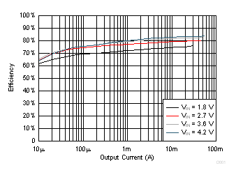
| VIN =1.8 V, 2.7 V, 3.6 V, 4.2 V | VOUT= 12 V |
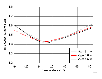
| VIN = 1.8 V, 3.6 V, 4.5 V | No switching |
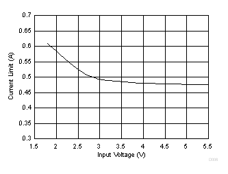
| VIN= 1.8 V to 5.5 V | TJ= 25°C |
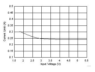
| VIN= 1.8 V to 5.5 V | TJ = 25°C |
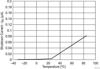
| VIN= 3.6 V into VIN Pin | TJ = –40°C to 85°C |
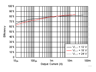
| VIN = 3.6 V | VOUT = 12 V, 18 V, 24 V |
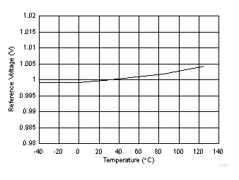
| VIN = 3.6 V | TJ= –40°C to 125°C |
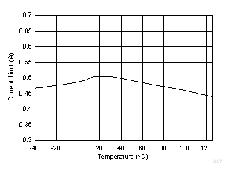
| VIN= 3.6 V | TJ = –40°C to 125°C |
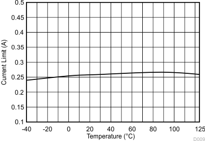
| VIN= 3.6 V | TJ = –40°C to 125°C |