SLVS873F June 2015 – September 2021 TPS61098 , TPS610981 , TPS610982 , TPS610985 , TPS610986 , TPS610987
PRODUCTION DATA
- 1 Features
- 2 Applications
- 3 Description
- 4 Revision History
- 5 Device Comparison Table
- 6 Pin Configuration and Functions
- 7 Specifications
- 8 Detailed Description
- 9 Applications and Implementation
- 10Power Supply Recommendations
- 11Layout
- 12Device and Documentation Support
- 13Mechanical, Packaging, and Orderable Information
Package Options
Mechanical Data (Package|Pins)
- DSE|6
Thermal pad, mechanical data (Package|Pins)
Orderable Information
9.2.1.2.3 Inductor Selection
Because the selection of the inductor affects steady state operation, transient behavior, and loop stability, the inductor is the most important component in power regulator design. There are three important inductor specifications, inductor value, saturation current, and dc resistance (DCR).
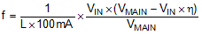
The TPS61098x is designed to work with inductor values between 2.2 µH and 4.7 µH. The inductance values affects the switching frequency ƒ in continuous current operation, which is proportional to 1/L as shown in Equation 4.
The inductor current ripple is fixed to 100mA typical value by internal design, but it can be affected by the inductor value indirectly. Normally when a smaller inductor value is applied, the inductor current ramps up and down more quickly, so the current ripple becomes bigger because the internal current comparator has some delay to respond. So if smaller inductor peak current is required in applications, a higher inductor value can be tried. However, the TPS61098x is optimized to work within a range of L and C combinations. The LC output filter inductance and capacitance must be considered together. The output capacitor sets the corner frequency of the converter while the inductor creates a Right-Half-Plane-Zero degrading the stability of the converter. Consequently with a larger inductor, a bigger capacitor normally should be used to ensure the same L/C ratio thus a stable loop.
Having selected an inductance value, the peak current for the inductor in steady-state operation varies as a function of the load, the input and output voltages and can be estimated using Equation 5.

where, 80% can be used for the boost converter power efficiency estimation, 100 mA is the typical inductor current ripple value and 50mA is half of the ripple value, which may be affected a little bit by inductor value. Equation 5 provides a suitable inductor current rating by using minimum input voltage, maximum boost output voltage and maximum load current for the calculation. Load transients and error conditions may cause higher inductor currents.
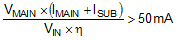
Equation 6 provides an easy way to estimate whether the device will work in continuous or discontinuous operation depending on the operating points. As long as the Equation 6 is true, continuous operation is typically established. If Equation 6 becomes false, discontinuous operation is typically established.
Selecting an inductor with insufficient saturation performance can lead to excessive peak current in the converter. This could eventually harm the device and reduce it's reliability.
In this example, the maximum load for the boost converter is 25 mA, and the minimum input voltage is 0.7 V, and the efficiency under this condition can be estimated at 80%, so the boost converter works in continuous operation by the calculation. The inductor peak current is calculated as 197 mA. To leave some margin, a 4.7 µH inductor with at least 250 mA saturation current is recommended for this application.
Table 9-1 also lists the recommended inductor for the TPS61098x device.
| INDUCTANCE [µH] | ISAT [A] | IRMS [A] | DC RESISTANCE [mΩ] | PART NUMBER | MANUFACTURER |
|---|---|---|---|---|---|
| 4.7 | 0.86 | 1.08 | 168 | VLF302510MT-4R7M | TDK |
| 4.7 | 0.57 | 0.95 | 300 | VLF252010MT-4R7M | TDK |
| 2.2 | 1.23 | 1.5 | 84 | VLF302510MT-2R2M | TDK |
| 2.2 | 0.83 | 0.92 | 120 | VLF252010MT-2R2M | TDK |