SLVS873F June   2015  – September 2021 TPS61098 , TPS610981 , TPS610982 , TPS610985 , TPS610986 , TPS610987

PRODUCTION DATA  

  1. Features
  2. Applications
  3. Description
  4. Revision History
  5. Device Comparison Table
  6. Pin Configuration and Functions
  7. Specifications
    1. 7.1 Absolute Maximum Ratings
    2. 7.2 ESD Ratings
    3. 7.3 Recommended Operating Conditions
    4. 7.4 Thermal Information
    5. 7.5 Electrical Characteristics
    6. 7.6 Typical Characteristics
  8. Detailed Description
    1. 8.1 Overview
    2. 8.2 Functional Block Diagrams
    3. 8.3 Feature Description
      1. 8.3.1 Boost Controller Operation
      2. 8.3.2 Pass-Through Operation
      3. 8.3.3 LDO / Load Switch Operation
      4. 8.3.4 Start Up and Power Down
      5. 8.3.5 Over Load Protection
      6. 8.3.6 Thermal Shutdown
    4. 8.4 Device Functional Modes
      1. 8.4.1 Operation Modes by MODE Pin
        1. 8.4.1.1 Active Mode
        2. 8.4.1.2 Low Power Mode
      2. 8.4.2 Burst Mode Operation under Light Load Condition
      3. 8.4.3 Pass-Through Mode Operation
  9. Applications and Implementation
    1. 9.1 Application Information
    2. 9.2 Typical Applications
      1. 9.2.1 VMAIN to Power MCU and VSUB to Power Subsystem
        1. 9.2.1.1 Design Requirements
        2. 9.2.1.2 Detailed Design Procedure
          1. 9.2.1.2.1 Device Choice
          2. 9.2.1.2.2 Maximum Output Current
          3. 9.2.1.2.3 Inductor Selection
          4. 9.2.1.2.4 Capacitor Selection
          5. 9.2.1.2.5 Control Sequence
        3. 9.2.1.3 Application Curves
      2. 9.2.2 VMAIN to Power the System in Low Power Mode
        1. 9.2.2.1 Design Requirements
        2. 9.2.2.2 Detailed Design Procedure
        3. 9.2.2.3 Application Curves
      3. 9.2.3 VSUB to Power the System in Active Mode
        1. 9.2.3.1 Design Requirements
        2. 9.2.3.2 Detailed Design Procedure
        3. 9.2.3.3 Application Curves
  10. 10Power Supply Recommendations
  11. 11Layout
    1. 11.1 Layout Guidelines
    2. 11.2 Layout Example
  12. 12Device and Documentation Support
    1. 12.1 Device Support
      1. 12.1.1 Third-Party Products Disclaimer
    2. 12.2 Documentation Support
      1. 12.2.1 Related Documentation
    3. 12.3 Receiving Notification of Documentation Updates
    4. 12.4 Support Resources
    5. 12.5 Trademarks
    6. 12.6 Electrostatic Discharge Caution
    7. 12.7 Glossary
  13. 13Mechanical, Packaging, and Orderable Information

Package Options

Mechanical Data (Package|Pins)
Thermal pad, mechanical data (Package|Pins)
Orderable Information
Maximum Output Current

For the boost converter, it provides output current for both V(MAIN) and V(SUB) rails. Its maximum output capability is determined by the input to output ratio and the current limit of the boost converter and can be estimated by Equation 3.
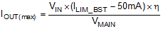
Equation 3. GUID-B8797F58-65D1-4695-A848-5E552DB4C314-low.gif

where

  • η is the boost converter power efficiency estimation
  • 50 mA is half of the inductor current ripple value

Minimum input voltage, maximum boost output voltage and minimum current limit ILIM_BST should be used as the worst case condition for the estimation.

Internal current limit is also implemented for the integrated LDO/load switch. So the maximum output current of VSUB rail should be lower than ILIM_SUB, which has 200 mA minimum value. For LDO version, the maximum output current is also limited by its input to output headroom, that is V(MAIN) - V(SUB). Make sure the headroom voltage is enough to support the load current. Please refer to Section 7.5 for the dropout voltage information.

In this example, assume the power efficiency is 80% (lower than typical value for the worst case estimation), so the calculated maximum output current of the boost converter is 50.9 mA, which satisfies the application requirements (15 mA + 10 mA). The load of VSUB rail is 10 mA, which is well below the V(SUB) rail current limit and the dropout voltage is also within the headroom.