SLVSBR3A May 2013 – June 2015 TPS61158
PRODUCTION DATA.
- 1 Features
- 2 Applications
- 3 Description
- 4 Revision History
- 5 Pin Configuration and Functions
- 6 Specifications
- 7 Detailed Description
- 8 Application and Implementation
- 9 Power Supply Recommendations
- 10Layout
- 11Device and Documentation Support
- 12Mechanical, Packaging, and Orderable Information
Package Options
Mechanical Data (Package|Pins)
- DRV|6
Thermal pad, mechanical data (Package|Pins)
- DRV|6
Orderable Information
8 Application and Implementation
NOTE
Information in the following applications sections is not part of the TI component specification, and TI does not warrant its accuracy or completeness. TI’s customers are responsible for determining suitability of components for their purposes. Customers should validate and test their design implementation to confirm system functionality.
8.1 Application Information
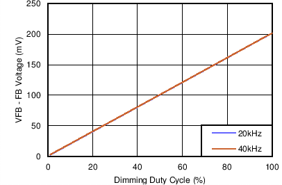
The TPS61158 provides a high-performance LED lighting solution for mobile handsets and other low power LCD backlit displays. The device can drive from 2 to 8 series LEDs in a compact and high efficient solution. An internal rectifying diode eliminates the need for an external Schottky. The LED current is controlled via a logic level PWM input with an internal low pass filter. This low pass filtered (analog) dimming, reduces the output capacitor requirement and provides noise free current control.
8.2 Typical Application
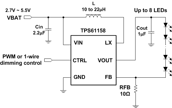 Figure 14. Typical Application for TPS61158
8.2.1 Design Requirements
For TPS61158 typical applications, use the parameters listed in Table 3 as the input parameters.
Table 3. Design Parameters
| DESIGN PARAMETER | EXAMPLE VALUE |
|---|---|
| Minimum input voltage | 2.7 V |
| Number of series LED | up to 8 |
| Switching frequency | 750 MHz |
8.2.2 Detailed Design Procedure
8.2.2.1 Inductor Selection
The selection of the inductor affects steady state operation as well as transient behavior, loop stability and the power conversion efficiency. These factors make it the most important component in power regulator design. There are three important inductor specifications, inductor value, DC resistance, and saturation current. Considering inductor value alone is not enough. The inductor value determines the inductor ripple current. Choose an inductor that can handle the necessary peak current without saturating, according to half of the peak-to-peak ripple current given by Equation 4, plus the inductor DC current given by:

Inductor values can have ±20% or even ±30% tolerance with no current bias. When the inductor current approaches saturation level, its inductance can decrease 20% to 35% from the 0A value depending on how the inductor vendor defines saturation. When selecting an inductor, please make sure its rated current, especially the saturation current, is larger than its peak current during the operation. Using an inductor with a smaller inductance value causes larger current ripple. This reduces the boost converter’s maximum output current, causes large input voltage ripple and reduces efficiency. Large inductance value provides much more output current and higher conversion efficiency. For these reasons, a 10-μH to 22-μH inductor value range is recommended. A 22-μH inductor optimizes the efficiency for most application while maintaining low inductor peak-to-peak ripple. Table 4 lists the recommended inductors for TPS61158. TPS61158 has built-in slope compensation to avoid sub-harmonic oscillation associated with current mode control. If the inductor value is lower than 10 μH, the slope compensation may not be adequate, and the loop can be unstable. Therefore, customers need to verify the inductor in their application if it is different from the recommended values.
Table 4. Recommended Inductors
| PART NUMBER | L (μH) | DCR MAX (mΩ) | SATURATION CURRENT (A) | Size (L x W x H mm) | VENDOR |
|---|---|---|---|---|---|
| LPS3015-103ML | 10 | 440 | 0.73 | 3.0 x 3.0 x 1.5 | Coilcraft |
| LPS3015-223ML | 22 | 825 | 0.5 | 3.0 x 3.0 x 1.5 | Coilcraft |
| 1229AS-H-100M | 10 | 288 | 0.75 | 3.5 x 3.7 x 1.2 | TOKO |
| 1229AS-H-220M | 22 | 672 | 0.5 | 3.5 x 3.7 x 1.2 | TOKO |
| VLS3012ET-100M | 10 | 336 | 0.64 | 3.0 x 3.0 x 1.2 | TDK |
| VLS3012ET-220M | 22 | 756 | 0.44 | 3.0 x 3.0 x 1.2 | TDK |
8.2.2.2 Maximum Output Current
The overcurrent limit in a boost converter limits the maximum input current and thus maximum input power for a given input voltage. Maximum output power is less than maximum input power due to power conversion losses. Therefore, the current limit setting, input voltage, output voltage and efficiency can all change maximum current output. The current limit clamps the peak inductor current; therefore, the ripple has to be subtracted to derive maximum DC current. The ripple current is a function of switching frequency, inductor value and duty cycle. The following equations take into account of all the above factors for maximum output current calculation.

where
- IP = inductor peak to peak ripple
- L = inductor value
- FS = switching frequency
- VOUT = output voltage of the boost converter. It is equal to the sum of VFB and the voltage drop across LEDs.
- VF = forward voltage of internal power diode. 0.75 V, typical

where
- IOUT_max = maximum output current of the boost converter
- ILIM = overcurrent limit
- η = boost efficiency (85%, typical)
To calculate the maximum output current in the worst case, use the minimum input voltage, maximum output voltage and maximum forward voltage of internal power diode (1 V). In order to leave enough design margin, the minimum current limit value 0.5 A, the minimum switching frequency 600 kHz, the inductor value with –30% tolerance, and a low power conversion efficiency, such as 80% or lower are recommended for the calculation. For instance, when minimum VIN is 3 V, 8 LEDs output equivalent to VOUT is 26 V, and the inductor is 22 µH, then the maximum output current is 33 mA in the worst case.
8.2.2.3 Input and Output Capacitor Selection
The output capacitor is mainly selected to meet the requirements for the output ripple and loop stability. This ripple voltage is related to the capacitor’s capacitance and its equivalent series resistance (ESR). Assuming a capacitor with zero ESR, the minimum capacitance needed for a given ripple can be calculated by

where
- Vripple = peak-to-peak output ripple.
The additional output ripple component caused by ESR is calculated using Equation 7:
Due to its low ESR, Vripple_ESR can be neglected for ceramic capacitors, but must be considered if tantalum or electrolytic capacitors are used.
Care must be taken when evaluating a ceramic capacitor’s derating under DC bias, aging and AC signal. The DC bias can significantly reduce capacitance. Ceramic capacitors can lose as much as 50% of its capacitance at its rated voltage. Therefore, leave the margin on the voltage rating to ensure adequate capacitance at the required output voltage.
The capacitor in the range of 1 μF to 10 μF is recommended for input side. The output requires a capacitor in the range of 0.47 μF to 2.2 μF. The output capacitor affects the loop stability of the boost regulator. If the output capacitor is below the range, the boost regulator can potentially become unstable.
The popular vendors for high value ceramic capacitors are:
TDK (http://www.component.tdk.com/components.php)
Murata (http://www.murata.com/cap/index.html)
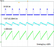
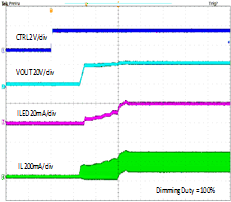
8.2.3 Application Curves
8.2.4 Additional Application Circuits
8.2.4.1 TPS61158 To Drive Up To 8 LEDs
Figure 23 shows a typical application for the TPS61158. This can drive from 2 to 8 series WLEDs.
 Figure 23. TPS61158 to Drive up to 8 LEDs
8.2.4.2 TPS61158 to Drive up to 8 LEDs with RC Filter at VIN Pin
Figure 24 is typical application circuit with RC filter at IN.
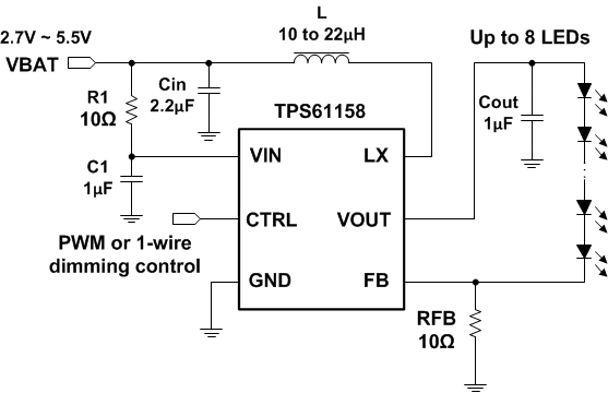 Figure 24. TPS61158 to Drive up to 8 LEDs With RC Filter at VIN Pin