SLVS789D November 2007 – December 2014 TPS61170
PRODUCTION DATA.
- 1 Features
- 2 Applications
- 3 Description
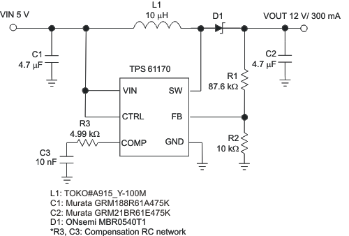
- 4 Typical Application Schematic
- 5 Revision History
- 6 Pin Configuration and Functions
- 7 Specifications
- 8 Detailed Description
- 9 Application and Implementation
- 10Power Supply Recommendations
- 11Layout
- 12Device and Documentation Support
- 13Mechanical, Packaging, and Orderable Information
Package Options
Mechanical Data (Package|Pins)
- DRV|6
Thermal pad, mechanical data (Package|Pins)
- DRV|6
Orderable Information
1 Features
- 3-V to 18-V Input Voltage Range
- High Output Voltage: Up to 38 V
- 1.2-A Integrated Switch
- 1.2-MHz Fixed Switching Frequency
- 12 V at 300 mA and 24 V at 150 mA From 5-V Input (Typical)
- Up to 93% Efficiency
- On-The-Fly Output Voltage Reprogramming
- Skip-Switching Cycle for Output Regulation at Light Load
- Built-in Soft Start
- 6-Pin, 2-mm × 2-mm QFN Package
2 Applications
- 5-V to 12-V and 24-V, 12-V to 24-V Boost Converter
- Buck Boost Regulation Using SEPIC Topology
- ADSL Modems
3 Description
The TPS61170 is a monolithic, high-voltage switching regulator with integrated 1.2-A, 40-V power MOSFET. The device can be configured in several standard switching-regulator topologies, including boost and SEPIC. The device has a wide input-voltage range to support applications with input voltage from multicell batteries or regulated 5-V, 12-V power rails.
The TPS61170 operates at a 1.2-MHz switching frequency, allowing the use of low-profile inductors and low-value ceramic input and output capacitors. External loop compensation components give the user flexibility to optimize loop compensation and transient response. The device has built-in protection features, such as pulse-by-pulse overcurrent limit, soft start, and thermal shutdown.
The FB pin regulates to a reference voltage of 1.229 V. The reference voltage can be lowered using a 1-wire digital interface (Easyscale™ protocol) through the CTRL pin. Alternatively, a pulse width-modulation (PWM) signal can be applied to the CTRL pin. The duty cycle of the signal reduces the feedback reference voltage proportionally.
The TPS61170 is available in a 6-pin 2-mm × 2-mm QFN package, allowing a compact power-supply solution.
Device Information(1)
| PART NUMBER | PACKAGE | BODY SIZE (NOM) |
|---|---|---|
| TPS61170 | VSON (6) | 2.00 mm x 2.00 mm |
- For all available packages, see the orderable addendum at the end of the datasheet.
4 Typical Application Schematic