SLVS789D November 2007 – December 2014 TPS61170
PRODUCTION DATA.
- 1 Features
- 2 Applications
- 3 Description
- 4 Typical Application Schematic
- 5 Revision History
- 6 Pin Configuration and Functions
- 7 Specifications
- 8 Detailed Description
- 9 Application and Implementation
- 10Power Supply Recommendations
- 11Layout
- 12Device and Documentation Support
- 13Mechanical, Packaging, and Orderable Information
Package Options
Mechanical Data (Package|Pins)
- DRV|6
Thermal pad, mechanical data (Package|Pins)
- DRV|6
Orderable Information
7 Specifications
7.1 Absolute Maximum Ratings
over operating free-air temperature range (unless otherwise noted) (1)| MIN | MAX | UNIT | ||
|---|---|---|---|---|
| VI | Supply Voltages on VIN (2) | –0.3 | 20 | V |
| Voltages on CTRL(2) | –0.3 | 20 | V | |
| Voltage on FB and COMP(2) | –0.3 | 3 | V | |
| Voltage on SW(2) | –0.3 | 40 | V | |
| TJ | Operating Junction Temperature | –40 | 150 | °C |
| Tstg | Storage temperature | –65 | 150 | °C |
(1) Stresses beyond those listed under absolute maximum ratings may cause permanent damage to the device. These are stress ratings only, and functional operation of the device at these or any other conditions beyond those indicated under Recommended Operating Conditions is not implied. Exposure to absolute-maximum-rated conditions for extended periods may affect device reliability.
(2) All voltage values are with respect to network ground terminal.
7.2 ESD Ratings
| VALUE | UNIT | |||
|---|---|---|---|---|
| V(ESD) | Electrostatic discharge | Human body model (HBM), per ANSI/ESDA/JEDEC JS-001(1) | ±2000 | V |
| Charged-device model (CDM), per JEDEC specification JESD22-C101(2) | ±750 | |||
(1) JEDEC document JEP155 states that 500-V HBM allows safe manufacturing with a standard ESD control process. Manufacturing with less than 500-V HBM is possible with the necessary precautions. Pins listed as ±2000 V may actually have higher performance.
(2) JEDEC document JEP157 states that 250-V CDM allows safe manufacturing with a standard ESD control process. Manufacturing with less than 250-V CDM is possible with the necessary precautions. Pins listed as ±750 V may actually have higher performance.
7.3 Recommended Operating Conditions
| MIN | TYP | MAX | UNIT | ||
|---|---|---|---|---|---|
| VI | Input voltage range, VIN | 3 | 18 | V | |
| VO | Output voltage range | VIN | 38 | V | |
| L | Inductor(1) | 10 | 22 | μH | |
| CI | Input capacitor | 1 | μF | ||
| CO | Output capacitor(1) | 1 | 10 | μF | |
| TA | Operating ambient temperature | –40 | 85 | °C | |
| TJ | Operating junction temperature | –40 | 125 | °C |
(1) These values are recommended values that have been successfully tested in several applications. Other values may be acceptable in other applications but should be fully tested by the user.
7.4 Thermal Information
| THERMAL METRIC(1) | TPS61170 | UNIT | |
|---|---|---|---|
| DRV | |||
| 6 PINS | |||
| RθJA | Junction-to-ambient thermal resistance | 66.5 | °C/W |
| RθJC(top) | Junction-to-case (top) thermal resistance | 85.6 | |
| RθJB | Junction-to-board thermal resistance | 36.0 | |
| ψJT | Junction-to-top characterization parameter | 1.7 | |
| ψJB | Junction-to-board characterization parameter | 36.4 | |
| RθJC(bot) | Junction-to-case (bottom) thermal resistance | 7.1 | |
(1) For more information about traditional and new thermal metrics, see the IC Package Thermal Metrics application report, SPRA953.
7.5 Electrical Characteristics
VIN = 3.6 V, CTRL = VIN, TA = –40°C to 85°C, typical values are at TA = 25°C (unless otherwise noted)| PARAMETER | TEST CONDITIONS | MIN | TYP | MAX | UNIT | |
|---|---|---|---|---|---|---|
| SUPPLY CURRENT | ||||||
| VI | Input voltage range, VIN | 3.0 | 18 | V | ||
| IQ | Operating quiescent current into VIN | Device PWM switching no load | 2.3 | mA | ||
| ISD | Shutdown current | CRTL=GND, VIN = 4.2 V | 1 | μA | ||
| UVLO | Under-voltage lockout threshold | VIN falling | 2.2 | 2.5 | V | |
| Vhys | Under-voltage lockout Hysteresis | 70 | mV | |||
| ENABLE AND REFERENCE CONTROL | ||||||
| V(CTRLh) | CTRL logic high voltage | VIN = 3 V to 18 V | 1.2 | V | ||
| V(CTRL) | CTRL logic low voltage | VIN = 3 V to 18 V | 0.4 | V | ||
| R(CTRL) | CTRL pulldown resistor | 400 | 800 | 1600 | kΩ | |
| toff | CTRL pulse width to shutdown | CTRL high to low | 2.5 | ms | ||
| tes_det | Easy Scale detection time(1) | CTRL pin low | 260 | μs | ||
| tes_delay | Easy Scale detection delay | 100 | μs | |||
| tes_win | Easy Scale detection window time | 1 | ms | |||
| VOLTAGE AND CURRENT CONTROL | ||||||
| VREF | Voltage feedback regulation voltage | 1.204 | 1.229 | 1.254 | V | |
| V(REF_PWM) | Voltage feedback regulation voltage under reprogram | VFB = 492 mV | 477 | 492 | 507 | mV |
| IFB | Voltage feedback input bias current | VFB = 1.229 V | 200 | nA | ||
| fS | Oscillator frequency | 1.0 | 1.2 | 1.5 | MHz | |
| Dmax | Maximum duty cycle | VFB = 100 mV | 90% | 93% | ||
| tmin_on | Minimum on pulse width | 40 | ns | |||
| Isink | Comp pin sink current | 100 | μA | |||
| Isource | Comp pin source current | 100 | μA | |||
| Gea | Error amplifier transconductance | 240 | 320 | 400 | μmho | |
| Rea | Error amplifier output resistance | 5 pF connected to COMP | 6 | MΩ | ||
| fea | Error amplifier crossover frequency | 5 pF connected to COMP | 500 | kHz | ||
| POWER SWITCH | ||||||
| RDS(on) | N-channel MOSFET on-resistance | VIN = 3.6 V | 0.3 | 0.6 | Ω | |
| VIN = 3.0 V | 0.7 | |||||
| ILN_NFET | N-channel leakage current | VSW = 35 V, TA = 25°C | 1 | μA | ||
| OC and SS | ||||||
| ILIM | N-Channel MOSFET current limit | D = Dmax | 0.96 | 1.2 | 1.44 | A |
| ILIM_Start | Start up current limit | D = Dmax | 0.7 | A | ||
| tHalf_LIM | Time step for half current limit | 5 | ms | |||
| tREF | Vref filter time constant | 180 | μs | |||
| tstep | VREF ramp up time | 213 | μs | |||
| EasyScale TIMING | ||||||
| tstart | Start time of program stream | 2 | μs | |||
| tEOS | End time of program stream | 2 | 360 | μs | ||
| tH_LB | High time low bit | Logic 0 | 2 | 180 | μs | |
| tL_LB | Low time low bit | Logic 0 | 2 × tH_LB | 360 | μs | |
| tH_HB | High time high bit | Logic 1 | 2 × tL_HB | 360 | μs | |
| tL_HB | Low time high bit | Logic 1 | 2 | 180 | μs | |
| VACKNL | Acknowledge output voltage low | Open drain, Rpullup =15 kΩ to Vin | 0.4 | V | ||
| tvalACKN | Acknowledge valid time | See (2) | 2 | μs | ||
| tACKN | Duration of acknowledge condition | See (2) | 512 | μs | ||
| THERMAL SHUTDOWN | ||||||
| Tshutdown | Thermal shutdown threshold | 160 | °C | |||
| Thysteresis | Thermal shutdown threshold hysteresis | 15 | °C | |||
(1) EasyScale communication is allowed immediately after the CTRL pin has been low for more than tes_det. To select EasyScale mode, the CTRL pin must be low for more than tes_det the end of tes_win.
(2) Acknowledge condition active 0, this condition will only be applied if the RFA bit is set. Open drain output, line needs to be pulled high by the host with resistor load.
7.6 Typical Characteristics
Table 1. Table Of Graphs
| Circuit of Figure 1, L = TOKO A915_Y-100M, D1 = ONsemi MBR0540T1, unless otherwise noted. | FIGURE | ||
|---|---|---|---|
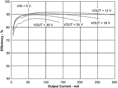
| Efficiency | VIN = 5 V; VOUT = 12 V, 18 V, 24 V, 30 V | Figure 1 | |
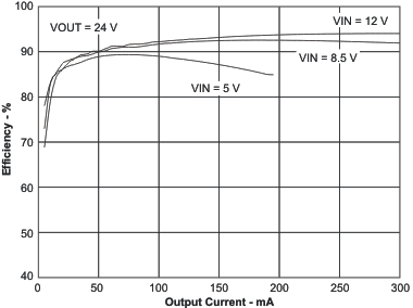
| Efficiency | VIN = 5 V, 8.5 V, 12 V; VOUT = 24 V | Figure 2 | |
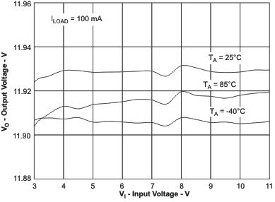
| Output voltage accuracy | ILOAD= 100 mA | Figure 3 | |
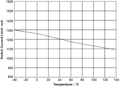
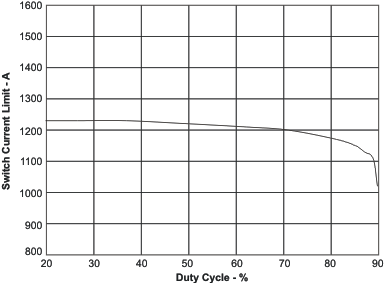
| Switch current limit | TA = 25°C | Figure 4 | |
| Switch current limit | Figure 5 | ||
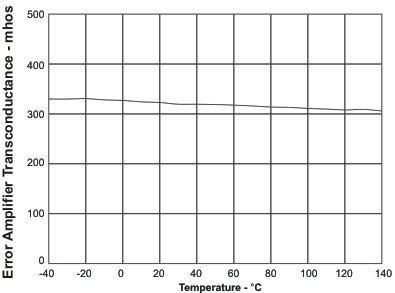
| Error amplifier transconductance | Figure 6 | ||
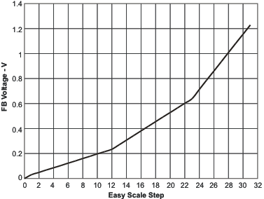
| EasyScale step | Figure 7 | ||
| PWM switching operation | VIN = 5 V; VOUT = 12 V; ILOAD= 250 mA | Figure 14 | |
| Load transient response | VIN = 5 V; VOUT = 12 V; ILOAD= 50 mA to 150 mA | Figure 15 | |
| Start-up | VIN = 5 V; VOUT = 12 V; ILOAD= 250 mA | Figure 16 | |
| Skip-cycle switching | VIN = 9 V ; VOUT = 12 V, ILOAD= 100 μA | Figure 17 | |