SLVS789D November 2007 – December 2014 TPS61170
PRODUCTION DATA.
- 1 Features
- 2 Applications
- 3 Description
- 4 Typical Application Schematic
- 5 Revision History
- 6 Pin Configuration and Functions
- 7 Specifications
- 8 Detailed Description
- 9 Application and Implementation
- 10Power Supply Recommendations
- 11Layout
- 12Device and Documentation Support
- 13Mechanical, Packaging, and Orderable Information
Package Options
Mechanical Data (Package|Pins)
- DRV|6
Thermal pad, mechanical data (Package|Pins)
- DRV|6
Orderable Information
8 Detailed Description
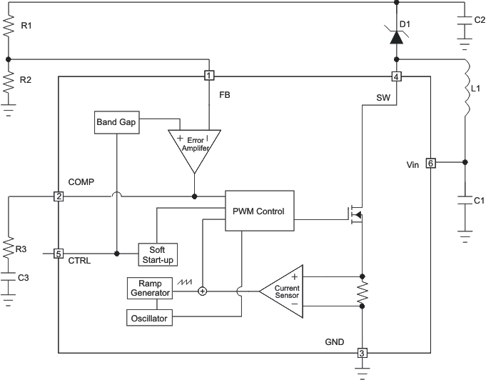
8.1 Overview
The TPS61170 integrates a 40-V low side FET for providing output voltages up to 38 V. The device regulates the output with current mode PWM (pulse width modulation) control. The switching frequency of the PWM is fixed at 1.2 MHz (typical). The PWM control circuitry turns on the switch at the beginning of each switching cycle. The input voltage is applied across the inductor and stores the energy as the inductor current ramps up. During this portion of the switching cycle, the load current is provided by the output capacitor. When the inductor current rises to the threshold set by the error amplifier output, the power switch turns off and the external Schottky diode is forward biased. The inductor transfers stored energy to replenish the output capacitor and supply the load current. This operation repeats each switching cycle. As shown in the block diagram, the duty cycle of the converter is determined by the PWM control comparator which compares the error amplifier output and the current signal.
A ramp signal from the oscillator is added to the current ramp. This slope compensation ramp is necessary to avoid subharmonic oscillations that are intrinsic to current mode control at duty cycles higher than 50%. The feedback loop regulates the FB pin to a reference voltage through an error amplifier. The output of the error amplifier must be connected to the COMP pin. An external RC compensation network must be connected to the COMP pin to optimize the feedback loop for stability and transient response.
8.2 Functional Block Diagram
8.3 Feature Description
8.3.1 Soft Start-Up
Soft-start circuitry is integrated into the IC to avoid a high inrush current during start-up. After the device is enabled by a logic high signal on the CTRL pin, the FB pin reference voltage ramps up in 32 steps, with each step taking 213 μs. This ensures that the output voltage rises slowly to reduce inrush current. Additionally, for the first 5 msec after the COMP voltage ramps, the current limit of the PWM switch is set to half of the normal current limit specification or below 700 mA (typical). See the start-up waveform for a typical example, Figure 16.
8.3.2 Overcurrent Protection
TPS61170 has a cycle-by-cycle overcurrent limit feature that turns off the power switch once the inductor current reaches the overcurrent limit. The PWM circuitry resets itself at the beginning of the next switch cycle. During an over-current event, this results in a decrease of output voltage that is directly proportional to load current. The current limit threshold as well as input voltage, output voltage, switching frequency and inductor value determine the maximum available output current. Larger inductance values typically increase the current output capability because of the reduced current ripple. See Maximum Output Current for the output current calculation.
8.3.3 Undervoltage Lockout (UVLO)
An undervoltage lockout prevents mis-operation of the device at input voltages below 2.2 V (typical). When the input voltage is below the undervoltage threshold, the device remains off and the internal switch FET is turned off. The undervoltage lockout threshold is set below minimum operating voltage of 3V to avoid any transient VIN dip triggering the UVLO and causing the device to reset. For the input voltages between UVLO threshold and 3 V, the device attempts operation, but the specifications are not ensured.
8.3.4 Thermal Shutdown
An internal thermal shutdown turns off the device when the typical junction temperature of 160°C is exceeded. The IC restarts when the junction temperature drops by 15°C.
8.3.5 Enable and Shutdown
The TPS61170 enters shutdown when the CTRL voltage is less than 0.4 V for more than 2.5 ms. In shutdown, the input supply current for the device is less than 1 μA (maximum). The CTRL pin has an internal 800-kΩ (typical) pulldown resistor to disable the device when the pin is left unconnected.
8.4 Device Functional Modes
8.4.1 Feedback Reference Program Mode Selection
The CTRL pin is used for changing the FB pin reference voltage on-the-fly. There are two methods to program the reference voltage, PWM signal and 1-wire interface (EasyScale). The programming mode is selected each time the device is enabled. The default mode is to use the duty cycle of the PWM signal on the CTRL pin to modulate the reference voltage. To enter the 1-wire interface mode, the following digital pattern on the CTRL pin must be recognized by the IC every time the IC starts from the shutdown mode.
- Pull CTRL pin high to enable the TPS61170 and to start the 1 wire mode detection window.
- After the EasyScale detection delay (tes_delay, 100 μsec) expires, drive CTRL low for more than the EasyScale detection time (tes_detect, 260 μsec).
- The CTRL pin has to be low for more than EasyScale detection time before the EasyScale detection window (tes_win, 1msec) expires. EasyScale detection window starts from the first CTRL pin low to high transition.
The IC immediately enters the 1-wire mode once the previous three conditions are met. The EasyScale communication can start before the detection window expires. Once the mode is programmed, it can not be changed without another start up. In other words, the IC must be shutdown by pulling the CTRL low for 2.5 ms and restarted in order to exit EasyScale Mode. See Figure 8 for a graphical explanation.
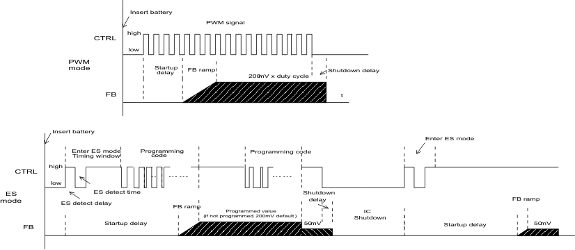 Figure 8. Mode Detection of Feedback Reference Program
8.4.2 PWM Program Mode
When the CTRL pin is constantly high, the FB voltage is regulated to 1.229V typically. However, the CTRL pin allows a PWM signal to lower this regulation voltage. The relationship between the duty cycle and FB voltage is given in Equation 1:
where
- Duty = duty cycle of the PWM signal
- 1.229 V = internal reference voltage
As shown in Figure 9, the IC chops up the internal 1.229 V reference voltage at the duty cycle of the PWM signal. The pulse signal is then filtered by an internal low pass filter. The output of the filter is connected to the error amplifier as the reference voltage for the FB pin regulation. The regulation voltage is independent of the PWM logic voltage level which often has large variations.
For optimum performance, use the PWM mode in the range of 5 kHz to 100 kHz. The requirement of minimum frequency comes from the EasyScale detection delay and detection time specification for the mode selection. The device can mistakenly enter 1 wire mode if the PWM signal frequency is less than 5 kHz. Because there is an internal fixed ON-time error of 40 nS, the FB voltage absolute value will be different than expected when the PWM frequency is above 100 kHz. For example, the additional duty cycle of 3.2% due to the ON-time error increases the FB voltage when using an 800 kHz PWM signal. A compromise between PWM frequency and FB voltage accuracy extends the frequency range. Adding an external RC filter to the pin serves no purpose.
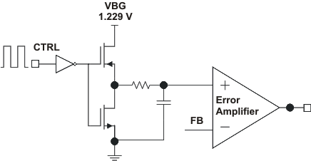 Figure 9. Block Diagram of Programmable FB Voltage Using PWM Signal
8.4.3 1-Wire Program Mode
The CTRL pin features a simple digital interface to control the feedback reference voltage. The 1-wire mode can save the processor power and battery life as it does not require a PWM signal all the time, and the processor can enter idle mode if available.
The TPS61170 adopts the EasyScale protocol, which can program the FB voltage to any of the 32 steps with single command. See Table 2 for the FB pin voltage steps. The programmed reference voltage is stored in an internal register. The default value is full scale when the device is first enabled (VFB = 1.229 V). A power reset clears the register value and reset it to default.
8.5 Programming
8.5.1 EasyScale
EasyScale is a simple but very flexible one pin interface to configure the FB voltage. The interface is based on a master-slave structure, where the master is typically a microcontroller or application processor. Figure 10 and Table 2 give an overview of the protocol. The protocol consists of a device specific address byte and a data byte. The device specific address byte is fixed to 72 hex. The data byte consists of five bits for information, two address bits, and the RFA bit. The RFA bit set to high indicates the Request for Acknowledge condition. The Acknowledge condition is only applied if the protocol was received correctly. The advantage of EasyScale compared with other on pin interfaces is that its bit detection is in a large extent independent from the bit transmission rate. It can automatically detect bit rates between 1.7 kBit/sec and up to 160 kBit/sec.
Table 2. Selectable FB Voltage
| FB VOLTAGE (mV) | D4 | D3 | D2 | D1 | D0 | |
|---|---|---|---|---|---|---|
| 0 | 0.000 | 0 | 0 | 0 | 0 | 0 |
| 1 | 0.031 | 0 | 0 | 0 | 0 | 1 |
| 2 | 0.049 | 0 | 0 | 0 | 1 | 0 |
| 3 | 0.068 | 0 | 0 | 0 | 1 | 1 |
| 4 | 0.086 | 0 | 0 | 1 | 0 | 0 |
| 5 | 0.104 | 0 | 0 | 1 | 0 | 1 |
| 6 | 0.123 | 0 | 0 | 1 | 1 | 0 |
| 7 | 0.141 | 0 | 0 | 1 | 1 | 1 |
| 8 | 0.160 | 0 | 1 | 0 | 0 | 0 |
| 9 | 0.178 | 0 | 1 | 0 | 0 | 1 |
| 10 | 0.197 | 0 | 1 | 0 | 1 | 0 |
| 11 | 0.215 | 0 | 1 | 0 | 1 | 1 |
| 12 | 0.234 | 0 | 1 | 1 | 0 | 0 |
| 13 | 0.270 | 0 | 1 | 1 | 0 | 1 |
| 14 | 0.307 | 0 | 1 | 1 | 1 | 0 |
| 15 | 0.344 | 0 | 1 | 1 | 1 | 1 |
| 16 | 0.381 | 1 | 0 | 0 | 0 | 0 |
| 17 | 0.418 | 1 | 0 | 0 | 0 | 1 |
| 18 | 0.455 | 1 | 0 | 0 | 1 | 0 |
| 19 | 0.492 | 1 | 0 | 0 | 1 | 1 |
| 20 | 0.528 | 1 | 0 | 1 | 0 | 0 |
| 21 | 0.565 | 1 | 0 | 1 | 0 | 1 |
| 22 | 0.602 | 1 | 0 | 1 | 1 | 0 |
| 23 | 0.639 | 1 | 0 | 1 | 1 | 1 |
| 24 | 0.713 | 1 | 1 | 0 | 0 | 0 |
| 25 | 0.787 | 1 | 1 | 0 | 0 | 1 |
| 26 | 0.860 | 1 | 1 | 0 | 1 | 0 |
| 27 | 0.934 | 1 | 1 | 0 | 1 | 1 |
| 28 | 1.008 | 1 | 1 | 1 | 0 | 0 |
| 29 | 1.082 | 1 | 1 | 1 | 0 | 1 |
| 30 | 1.155 | 1 | 1 | 1 | 1 | 0 |
| 31 | 1.229 | 1 | 1 | 1 | 1 | 1 |
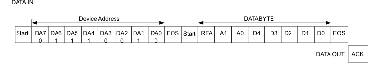 Figure 10. EasyScale Protocol Overview
Table 3. EasyScale Bit Description
| BYTE | BIT NUMBER | NAME | TRANSMISSION DIRECTION | DESCRIPTION |
|---|---|---|---|---|
| Device Address Byte 72 hex |
7 | DA7 | IN | 0 MSB device address |
| 6 | DA6 | 1 | ||
| 5 | DA5 | 1 | ||
| 4 | DA4 | 1 | ||
| 3 | DA3 | 0 | ||
| 2 | DA2 | 0 | ||
| 1 | DA1 | 1 | ||
| 0 | DA0 | 0 LSB device address | ||
| Data byte | 7 (MSB) | RFA | IN | Request for acknowledge. If high, acknowledge is applied by device |
| 6 | A1 | 0 Address bit 1 | ||
| 5 | A0 | 0 Address bit 0 | ||
| 4 | D4 | Data bit 4 | ||
| 3 | D3 | Data bit 3 | ||
| 2 | D2 | Data bit 2 | ||
| 1 | D1 | Data bit 1 | ||
| 0 (LSB) | D0 | Data bit 0 | ||
| ACK | OUT | Acknowledge condition active 0, this condition will only be applied in case RFA bit is set. Open-drain output, Line must be pulled high by the host with a pullup resistor. This feature can only be used if the master has an open-drain output stage. In case of a push pull output stage Acknowledge condition may not be requested! |
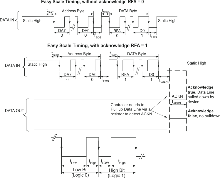 Figure 11. EasyScale— Bit Coding
All bits are transmitted MSB first and LSB last. Figure 11 shows the protocol without acknowledge request (Bit RFA = 0), Figure 11 with acknowledge (Bit RFA = 1) request. Prior to both bytes, device address byte and data byte, a start condition must be applied. For this, the CTRL pin must be pulled high for at least tstart (2 μs) before the bit transmission starts with the falling edge. If the CTRL pin is already at high level, no start condition is needed prior to the device address byte. The transmission of each byte is closed with an End of Stream condition for at least tEOS (2 μs).
The bit detection is based on a Logic Detection scheme, where the criterion is the relation between tLOW and tHIGH. It can be simplified to:
High Bit: tHIGH > tLOW, but with tHIGH at least 2x tLOW, see Figure 11.
Low Bit: tHIGH < tLOW, but with tLOW at least 2x tHIGH, see Figure 11.
The bit detection starts with a falling edge on the CTRL pin and ends with the next falling edge. Depending on the relation between tHIGH and tLOW, the logic 0 or 1 is detected.
The acknowledge condition is only applied if:
- Acknowledge is requested by a set RFA bit.
- The transmitted device address matches with the device address of the device.
- 16 bits is received correctly.
If the device turns on the internal ACKN-MOSFET and pulls the CTRL pin low for the time tACKN, which is 512 μs maximum then the Acknowledge condition is valid after an internal delay time tvalACK. This means that the internal ACKN-MOSFET is turned on after tvalACK, when the last falling edge of the protocol was detected. The master controller keeps the line low in this period. The master device can detect the acknowledge condition with its input by releasing the CTRL pin after tvalACK and read back a logic 0. The CTRL pin can be used again after the acknowledge condition ends.
Note that the acknowledge condition may only be requested if the master device has an open-drain output. For the push-pull output stage, the use a series resistor in the CRTL line to limit the current to 500 μA is recommended for such cases as:
- an accidentally requested acknowledge, or
- to protect the internal ACKN-MOSFET.