SLVSA85E June 2010 – December 2016 TPS61187
PRODUCTION DATA.
- 1 Features
- 2 Applications
- 3 Description
- 4 Revision History
- 5 Pin Configuration and Functions
- 6 Specifications
-
7 Detailed Description
- 7.1 Overview
- 7.2 Functional Block Diagram
- 7.3 Feature Description
- 7.4
Device Functional Modes
- 7.4.1 Brightness Dimming Control
- 7.4.2 Adjustable PWM Dimming Frequency and Mode Selection (R_FPWM/MODE)
- 7.4.3 Mode Selection - Phase-Shift PWM Or Direct PWM Dimming
- 7.4.4 Overvoltage Clamp and Voltage Feedback (OVC / FB)
- 7.4.5 Current-Sink Open Protection
- 7.4.6 Overcurrent and Short-Circuit Protection
- 7.4.7 Thermal Protection
- 8 Application and Implementation
- 9 Power Supply Recommendations
- 10Layout
- 11Device and Documentation Support
- 12Mechanical, Packaging, and Orderable Information
Package Options
Mechanical Data (Package|Pins)
- RTJ|20
Thermal pad, mechanical data (Package|Pins)
- RTJ|20
Orderable Information
8 Application and Implementation
NOTE
Information in the following applications sections is not part of the TI component specification, and TI does not warrant its accuracy or completeness. TI’s customers are responsible for determining suitability of components for their purposes. Customers should validate and test their design implementation to confirm system functionality.
8.1 Application Information
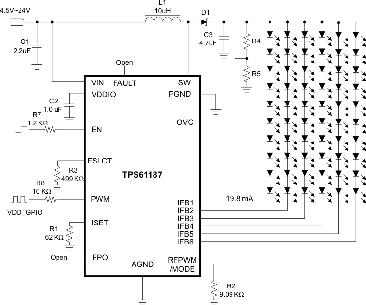
The TPS61187 provides a high-performance LED lighting solution for tablets, notebooks, monitors, and a variety of industrial designs. The device can drive 6 strings of 10 series LEDs in a compact and highly efficient solution. The TPS61187 provides a gate driver to an external P-channel MOSFET, which can be turned off during device shutdown or fault condition.
8.2 Typical Application
 Figure 17. TPS61187 Typical Application
8.2.1 Design Requirements
For typical WLED-driver applications, use the parameters listed in Table 3.
Table 3. Design Parameters
| DESIGN PARAMETER | EXAMPLE VALUE |
|---|---|
| Input voltage | 4 V to 24 V |
| Output voltage | 38 V (maximum) |
| LED string current | 30 mA (maximum) |
| Switching frequency | 280 kHz to 1 MHz |
8.2.2 Detailed Design Procedure
8.2.2.1 Inductor Selection
Because selection of the inductor affects power supply steady state operation, transient behavior, and loop stability, the inductor is the most important component in switching power regulator design. There are three specifications most important to the performance of the inductor: inductor value, DC resistance (DCR), and saturation current. The TPS61187 is designed to work with inductor values between 10 µH and 47 µH. A 10-µH inductor is typically available in a smaller or lower profile package, while a 47-µH inductor may produce higher efficiency due to a slower switching frequency and/or lower inductor ripple. If the boost output current is limited by the over-current protection of the device, using a 10-µH inductor and the highest switching frequency maximizes controller output current capability.
Internal loop compensation for PWM control is optimized for the external component values, including typical tolerances, recommended in Table 4. Inductor values can have ±20% tolerance with no current bias. When the inductor current approaches saturation level, its inductance can decrease 20% to 35% from the 0-A value depending on how the inductor vendor defines saturation. In a boost regulator, the inductor dc current can be calculated with Equation 6.

where
- VOUT = boost output voltage
- IOUT = boost output current
- VIN = boost input voltage
- η = power conversion efficiency, use 90% for TPS61187 applications
The inductor current peak-to-peak ripple can be calculated with Equation 7.

where
- IPP = inductor peak-to-peak ripple
- L = inductor value
- FS = Switching frequency
- VOUT = boost output voltage
- VIN = boost input voltage
Therefore, the peak current seen by the inductor is calculated with Equation 8.

Select an inductor with a saturation current over the calculated peak current. To calculate the worst-case inductor peak current, use the minimum input voltage, maximum output voltage, and maximum load current.
Regulator efficiency is dependent on the resistance of its high current path and switching losses associated with the PWM switch and power diode. Although the TPS61187 device has optimized the internal switch resistances, the overall efficiency is affected by the inductor DCR. Lower DCR improves efficiency. However, there is a trade off between DCR and inductor footprint; furthermore, shielded inductors typically have higher DCR than unshielded ones. Table 4 lists the recommended inductors.
Table 4. Recommended Inductor For TPS61187
| L (µH) | DCR (mΩ) | ISAT (A) | SIZE (L × W × H mm) | |
| TOKO | ||||
| A915AY – 4R7M | 4.7 | 38 | 1.87 | 5.2 × 5.2 × 3.0 |
| A915AY – 100M | 10 | 75 | 1.24 | 5.2 × 5.2 × 3.0 |
| TDK | ||||
| SLF6028T – 4R7N1R6 | 4.7 | 38 | 1.87 | 5.2 × 5.2 × 3.0 |
| SLF6028T – 4R7N1R6 | 10 | 75 | 1.24 | 5.2 × 5.2 × 3.0 |
8.2.2.2 Output Capacitor Selection
The output capacitor is mainly selected to meet the requirement for output ripple and loop stability. This ripple voltage is related to the capacitance of the capacitor and its equivalent series resistance (ESR). Assuming a capacitor with zero ESR, the minimum capacitance needed for a given ripple can be calculated with Equation 9:

where
- Vripple = peak-to-peak output ripple
The additional part of the ripple caused by ESR is calculated using: Vripple_ESR = IOUT × RESR
Due to its low ESR, Vripple_ESR can be neglected for ceramic capacitors, but must be considered if tantalum or electrolytic capacitors are used. The controller output voltage also ripples due to the load transient that occurs during PWM dimming. The TPS61187 adopts a patented technology to limit this type of output ripple even with the minimum recommended output capacitance. In a typical application, the output ripple is less than 250 mV during PWM dimming with a 4.7-µF output capacitor. However, the output ripple decreases with higher output capacitances.
8.2.2.3 Isolation FET Selection
The TPS61187 provides a gate driver to an external P-channel MOSFET, which can be turned off during device shutdown or fault condition. This MOSFET can provide a true shutdown function and also protect the battery from output short-circuit conditions. The source of the PMOS must be connected to the input, and a pullup resistor is required between the source and gate of the FET to keep the FET off during device shutdown. To turn on the isolation FET, the FAULT pin is pulled low and clamped at 8 V below the VBAT pin voltage. During device shutdown or fault condition, the isolation FET is turned off, and the input voltage is applied on the isolation MOSFET. During a short-circuit condition, the catch diode (D2 in the typical application circuit) is forward biased when the isolation FET is turned off. The drain of the isolation FET swings below ground. The voltage across the isolation FET can be momentarily greater than the input voltage. Therefore, select a 30-V PMOS for a 24-V maximum input. The on resistance of the FET has a large impact on power conversion efficiency since the FET carries the input voltage. Select a MOSFET with Rds(on) less than 100 mΩ to limit the power losses.


