SLVSA85E June 2010 – December 2016 TPS61187
PRODUCTION DATA.
- 1 Features
- 2 Applications
- 3 Description
- 4 Revision History
- 5 Pin Configuration and Functions
- 6 Specifications
-
7 Detailed Description
- 7.1 Overview
- 7.2 Functional Block Diagram
- 7.3 Feature Description
- 7.4
Device Functional Modes
- 7.4.1 Brightness Dimming Control
- 7.4.2 Adjustable PWM Dimming Frequency and Mode Selection (R_FPWM/MODE)
- 7.4.3 Mode Selection - Phase-Shift PWM Or Direct PWM Dimming
- 7.4.4 Overvoltage Clamp and Voltage Feedback (OVC / FB)
- 7.4.5 Current-Sink Open Protection
- 7.4.6 Overcurrent and Short-Circuit Protection
- 7.4.7 Thermal Protection
- 8 Application and Implementation
- 9 Power Supply Recommendations
- 10Layout
- 11Device and Documentation Support
- 12Mechanical, Packaging, and Orderable Information
Package Options
Mechanical Data (Package|Pins)
- RTJ|20
Thermal pad, mechanical data (Package|Pins)
- RTJ|20
Orderable Information
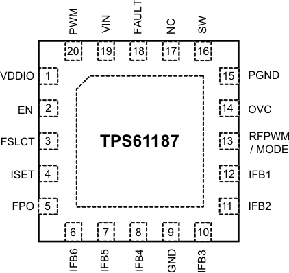
5 Pin Configuration and Functions
RTJ Package
20-Pin QFN With Thermal Pad
Top View

Pin Functions
| PIN | TYPE | DESCRIPTION | |
|---|---|---|---|
| NO. | NAME | ||
| 1 | VDDIO | A | Internal pre-regulator. Connect a 1-µF ceramic capacitor to VDDIO. |
| 2 | EN | I | Enable |
| 3 | FSLCT | I | Switching frequency selection pin. Use a resistor to set the frequency between 300 kHz to 1 MHz. |
| 4 | ISET | I | Full-scale LED current set pin. Connecting a resistor to the pin programs the current level. |
| 5 | FPO | O | Fault protection output to indicate fault conditions including OVP, OC, and OT. |
| 6, 7, 8, 10,11,12 |
IFB1 to IFB6 | A | Regulated current sink input pins |
| 9, | GND | G | Analog ground |
| 13 | RFPWM / MODE | I | Dimming frequency program pin with an external resistor / mode selection, see(1) |
| 14 | OVC | A | Overvoltage clamp pin / voltage feedback, see(1) |
| 15 | PGND | G | Power ground |
| 16 | SW | A | Drain connection of the internal power FET |
| 17 | NC | — | No connection |
| 18 | FAULT | O | Fault pin to drive external ISO FET |
| 19 | VIN | A | Supply input pin |
| 20 | PWM | I | PWM signal input pin |
| — | Thermal Pad | — | Connect to GND plane for better thermal performance. |
| A: Analog; G: Ground; I: Input: O: Output; P: Power | |||
(1) See Application and Implementation for details.