SLVSBG1D October 2012 – May 2015 TPS61196
PRODUCTION DATA.
- 1 Features
- 2 Applications
- 3 Description
- 4 Revision History
- 5 Pin Configuration and Functions
- 6 Specifications
-
7 Detailed Description
- 7.1 Overview
- 7.2 Functional Block Diagram
- 7.3 Feature Description
- 7.4
Device Functional Modes
- 7.4.1
Protections
- 7.4.1.1 Switch Current Limit Protection Using the ISNS Pin
- 7.4.1.2 LED Open Protection
- 7.4.1.3 LED Short-Cross Protection Using the FBP Pin
- 7.4.1.4 Schottky Diode Open Protection
- 7.4.1.5 Schottky Diode Short Protection
- 7.4.1.6 IFB Overvoltage Protection During Start-up
- 7.4.1.7 Output Overvoltage Protection Using the OVP Pin
- 7.4.1.8 Output Short-to-Ground Protection
- 7.4.1.9 IFB Short-to-Ground Protection
- 7.4.1.10 ISET Short-to-Ground Protection
- 7.4.1.11 Thermal Protection
- 7.4.2 Indication For Fault Conditions
- 7.4.1
Protections
- 8 Application and Implementation
- 9 Power Supply Recommendations
- 10Layout
- 11Device and Documentation Support
- 12Mechanical, Packaging, and Orderable Information
Package Options
Mechanical Data (Package|Pins)
- PWP|28
Thermal pad, mechanical data (Package|Pins)
- PWP|28
Orderable Information
7 Detailed Description
7.1 Overview
The TPS61196 provides a highly integrated solution for LCD TV backlight with an independent PWM dimming function for each string. This device is a current mode boost controller driving up to six WLED strings with multiple LEDs in series. Each string has an independent current regulator providing a LED current adjustable from 50 mA to 400 mA within ±1.5% matching accuracy. The minimal voltage at the current sink is programmable in the range of 0.3 V to 1 V to fit with different LED current settings. The input voltage range for the device is from 8 V to 30 V.
7.2 Functional Block Diagram
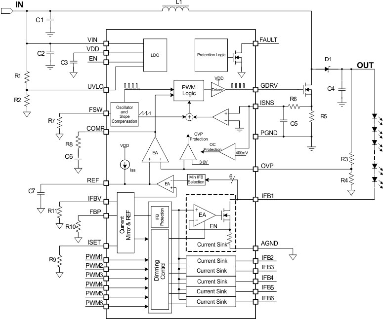
7.3 Feature Description
7.3.1 Supply Voltage
The TPS61196 has a built-in linear regulator to supply the device analog and logic circuitry. The VDD pin, output of the regulator, must be connected to a 1-µF bypass capacitor. VDD only has a current sourcing capability of 15 mA. VDD voltage is ready after the EN pin is pulled high.
7.3.2 Boost Controller
The TPS61196 regulates the output voltage with current mode pulse width modulation (PWM) control. The control circuitry turns on an external switch FET at the beginning of each switching cycle. The input voltage is applied across the inductor and stores the energy as the inductor current ramps up. During this portion of the switching cycle, the load current is provided by the output capacitor. When the inductor current rises to the threshold set by the Error Amplifier (EA) output, the switch FET is turned off and the external Schottky diode is forward biased. The inductor transfers stored energy to replenish the output capacitor and supply the load current. This operation repeats each switching cycle. The switching frequency is programmed by an external resistor.
A ramp signal from the oscillator is added to the current ramp to provide slope compensation, shown in Figure 23. The duty cycle of the converter is then determined by the PWM Logic block which compares the EA output and the slope compensated current ramp. The feedback loop regulates the OVP pin to a reference voltage generated by the minimum voltage across the IFB pins. The output of the EA is connected to the COMP pin. An external RC compensation network must be connected to the COMP pin to optimize the feedback loop for stability and transient response.
The TPS61196 consistently adjusts the boost output voltage to account for any changes in LED forward voltages. In the event that the boost controller is not able to regulate the output voltage due to the minimum pulse width (ton(min), in the Electrical Characteristics), the TPS61196 enters pulse skip mode. In this mode, the device keeps the power switch off for several switching cycles to prevent the output voltage from rising above the regulated voltage. This operation typically occurs in light load condition or when the input voltage is higher than the output voltage.
7.3.3 Switching Frequency
The switching frequency is programmed between 100 kHz to 800 kHz by an external resistor (R9 in Figure 23). To determine the resistance by a given frequency, use the curve in Figure 4 or calculate the resistance value by Equation 1. Table 1 shows the recommended resistance values for some switching frequencies.

7.3.4 Enable and Undervoltage Lockout
The TPS61196 is enabled with the soft start-up when the EN pin voltage is higher than 1.8 V. A voltage of less than 1 V disables the device.
An undervoltage lockout (UVLO) protection feature is provided. When the voltage at the VIN pin is less than 6.5 V, the TPS61196 is powered off. The TPS61196 resumes the operation once the voltage at the VIN pin recovers above the hysteresis (VVIN_HYS) more than the UVLO threshold of input falling voltage. If a higher UVLO voltage is required, use the UVLO pin as shown in Figure 19 to adjust the input UVLO threshold by using an external resistor divider. Once the voltage at the UVLO pin exceeds the 1.229-V threshold, the device is powered on, and a hysteresis current source of 3.9 µA is added. When the voltage at the UVLO pin drops lower than 1.229 V, the current source is removed. The resistors of R1, R2, and R5 can be calculated by Equation 2 from required VSTART and VSTOP. To avoid noise coupling, the resistor divider R1 and R2 must be close to the UVLO pin. Placing a filter capacitor of more than 10 nF as shown in Figure 19 can eliminate the impact of the switching ripple and improve the noise immunity.
If the UVLO function is not used, pull up the UVLO pin to the VDD pin.
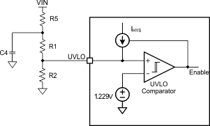 Figure 19. Undervoltage Lockout Circuit
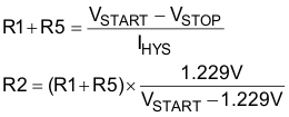
where
- IHYS is 3.9 µA sourcing current from the UVLO pin.
When the UVLO condition happens, the FAULT pin outputs high impedance. As long as the UVLO condition removes, the FAULT pin outputs low impedance.
7.3.5 Power-up Sequencing and Soft Start-up
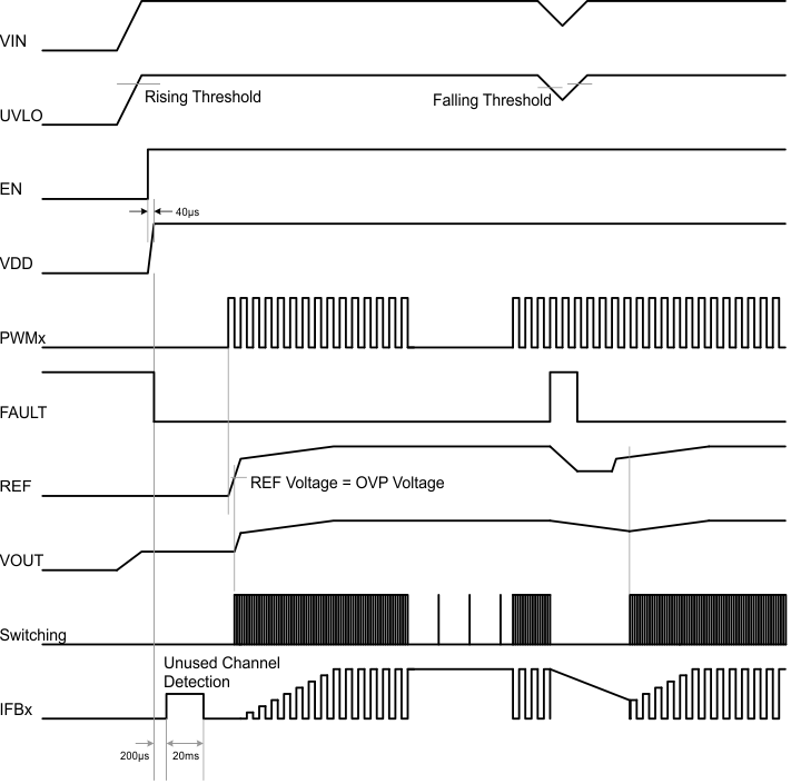
The input voltage, UVLO pin voltage, EN input signal and the input dimming PWM signal control the power up of the TPS61196. After the input voltage is above the required minimal input voltage of 7.5 V, the internal circuit is ready to be powered up. After the UVLO pin is above the threshold of 1.229 V and the EN signal is high, the internal LDO and logic circuit are activated. The device outputs a 20-ms pulse to detect the unused channels and remove them from the control loop. When any PWM dimming signal is high, the soft start-up begins. If the PWM dimming signals come before the EN signal is high, the soft start-up begins immediately after the detection of unused channels.
The TPS61196 has integrated the soft-start circuitry working with an external capacitor at the REF pin to avoid inrush current during start-up. During the start-up period, the capacitor at the REF pin is charged with a soft-start current source. When the REF pin voltage is higher than the output feedback voltage at the OVP pin, the boost controller starts switching and the output voltage starts to ramp up. At the same time, the LED current sink starts to drive the LED strings. At the beginning of the soft start, the charge current is 200 µA. Once the voltage of the REF pin exceeds 2 V, the charge current changes to 10 µA and continues to charge the capacitor. When the current sinks are driving the LED strings, the IFB voltages are monitored. When the minimum IFB voltage is above 200 mV less than the setting voltage at the IFBV pin, the charge current is stopped, and the soft start-up is finished. The TPS61196 enters normal operation to regulate the minimum IFB voltage to the required voltage set by the resistor at the IFBV pin. The total soft start time is determined by the external capacitance. The capacitance must be within 1 µF to 4.7 µF for different start-up time and different output voltage.
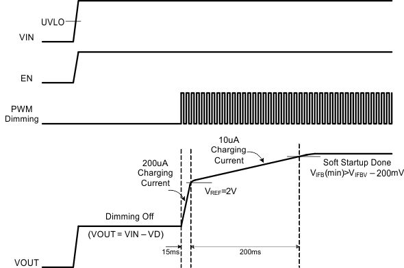 Figure 21. Soft-Start Waveforms
7.3.6 Unused LED String
If the application requires less than six LED strings, the TPS61196 simply requires connecting the unused IFB pin to ground through a resistor between 20 kΩ and 36 kΩ. Once the TPS61196 is turned on, the TPS61196 uses a 60-µA current source to detect the IFB pin voltage. If the IFB voltage is between 1 V and 2.5 V, the device immediately disables this string during start-up.
7.3.7 Current Regulation
The six channel current sink regulators can be configured to provide up to 400 mA per string. The expected LED current is programmed by a resistor (R11 in Figure 23) at the ISET using Equation 3.

where
- VISET is the ISET pin voltage of 1.229 V
- KISET is the current multiple of 3992.
To sink the set LED current, the current sink regulator requires a minimum headroom voltage at the IFB pins for working properly. For example, when the LED current is set to 130 mA, the minimum voltage required at the IFB pin must be higher than 0.35 V. For other LED currents, refer to Figure 5 for recommended minimum headroom voltage required. The TPS61196 regulates the minimum voltage of the IFB pins to the IFBV voltage. The IFBV voltage is adjustable with an external resistor (R10 in the Figure 23) at the IFBV pin. After choosing the minimum IFB voltage, the IFBV voltage must be set to this value and the setting resistance can be calculated by Equation 4.

If a large LED current is set, the headroom voltage is required higher. This leads to more heat on the device. To maintain the total power dissipation in the range of the package limit, normally all strings can not sink large current in continuous mode but pulse mode. The backlight of an active shutter glass 3-D TV may work with large LED current in pulse mode.
7.3.8 PWM Dimming
LED brightness dimming is set by applying an external PWM signal of 90 Hz to 22 kHz to the PWM pins. Each LED string has an independent PWM input. Varying the PWM duty cycle from 0% to 100% adjusts the LED from minimum to maximum brightness respectively. The recommended minimum on time of the LED string is 10 µsec. Thus, the device has a minimum dimming duty cycle of 500:1 at 200 Hz.
When all PWM voltages are pulled low during dimming off, the TPS61196 turns off the LED strings and keeps the boost converter running at PFM mode. The output voltage is kept at the level which is a little bit lower than that when PWM is high. Thus, the device limits the output ripple due to the load transient that occurs during PWM dimming.
When all PWM voltages are pulled low for more than 20 ms, to avoid the REF pin voltage dropping due to the leakage current, the voltage of the REF pin is held by an internal reference voltage which equals to the REF pin voltage in normal dimming operation. Thus, the output voltage will be kept at the same level as the normal output voltage.
Since the output voltage in long time dimming off status is almost the same as the normal voltage for turning the LED on, the TPS61196 turns on the LED very fast without any flicker when recovering from long time dimming off to small duty cycle dimming on.
7.4 Device Functional Modes
7.4.1 Protections
The TPS61196 has a full set of protections making the system safe to any abnormal conditions. Some protections will latch the TPS61196 in off state until its power supply is recycled or it is disabled and then enabled again. In latch off state, the REF pin voltage is discharged to 0 V.
7.4.1.1 Switch Current Limit Protection Using the ISNS Pin
The TPS61196 monitors the inductor current through the voltage across a sense resistor (R7 in the Figure 23) in order to provide current limit protection. During the switch FET on period, when the voltage at the ISNS pin rises above 400 mV (VISNS in the Electrical Characteristics table), the TPS61196 turns off the FET immediately and does not turn it back on until the next switch cycle. The switch current limit is equal to 400 mV / R7.
7.4.1.2 LED Open Protection
When one of the LED strings is open, the voltage at the IFB pin connecting to this LED string drops to zero during dimming-on time. The TPS61196 monitors the IFB voltage for 20 ms. If the IFB voltage is still below the threshold of 0.2 V, the current sink is disabled and an internal pull-up current is activated to detect the IFB voltage again. If the IFB voltage is pulled up to a high voltage, this LED string is recognized as LED open. As a result, the device deactivates the open IFB pin and removes it from the voltage feedback loop. Afterwards, the output voltage returns to the voltage required for the connected LED strings. The IFB pin currents of the connected strings remain in regulation during this process. If all the LED strings are open, the TPS61196 is latched off.
7.4.1.3 LED Short-Cross Protection Using the FBP Pin
If one or several LEDs short in one string, the corresponding IFB pin voltage rises but continues to sink the LED current, causing increased device power dissipation. To protect the device, the TPS61196 provides a programmable LED short-across protection feature by properly sizing the resistor on the FBP pin (R12 in Figure 23) using Equation 5.

If any IFB pin voltage exceeds the threshold (VLED_SHORT), the device turns off the corresponding current sink and removes this IFB pin from the output voltage regulation loop. Current regulation of the remaining IFB pins is not affected.
7.4.1.4 Schottky Diode Open Protection
When the device is powered on, it checks the topology connection first. After the TPS61196 delays 400 µs, it checks the voltage at the OVP pin to see if the Schottky diode is not connected or the boost output is hard-shorted to ground. If the voltage at the OVP pin is lower than 70 mV, the TPS61196 is locked in off state until the input power is recycled or it is enabled again.
7.4.1.5 Schottky Diode Short Protection
If the rectifier Schottky diode is shorted, the reverse current from output capacitor to ground is very large when the switcher MOSFET is turned on. Because the current mode control topology has a minimum edge blanking time to immunize against the spike current through the switcher, if the parasite inductance between the output capacitor through the switcher to ground is zero, the external MOSFET will be damaged in this short period due to the huge power dissipation in this case. But with a small parasite inductance, the power dissipation is limited. The boost converter works in minimum pulse width in this situation due to cycle by cycle over-current protection. The output voltage drops and the all-string-open protection is triggered because of the low voltage at all IFB pins. The TPS61196 is latched off.
7.4.1.6 IFB Overvoltage Protection During Start-up
When any of IFB pins reaches the threshold (VOVP_IFB) of 38 V during start-up, the device stops switching and stays in latch-off immediately to protect from damage. In latch-off state, the REF pin voltage is discharged.
7.4.1.7 Output Overvoltage Protection Using the OVP Pin
Use a resistor divider to program the maximum output voltage of the boost converter. To ensure the LED string can be turned on with setting current, the maximum output voltage must be higher than the forward voltage drop of the LED string. The maximum required voltage can be calculated by multiplying the maximum LED forward voltage (VFWD(max)) and number (n) of series LEDs , and adding extra 1 V to account for regulation and resistor tolerances and load transients.
The recommended bottom feedback resistor of the resistor divider (R4 in Figure 23) is 10 kΩ. Calculate the top resistor (R3 in the Figure 23) using Equation 6, where VOVP is the maximum output voltage of the boost converter.

When the device detects that the voltage at the OVP pin exceeds overvoltage protection threshold of 3.02 V, indicating that the output voltage has exceeded the clamp threshold voltage, the TPS61196 clamps the output voltage to the set threshold. When the OVP pin voltage does not drop from the OVP threshold for more than 500 ms, the device is latched off until the input power or the EN pin voltage is re-cycled.
7.4.1.8 Output Short-to-Ground Protection
When the inductor peak current reaches twice the switch current limit in each switching cycle, the device immediately disables the boost controller until the fault is cleared. This protects the device and external components from damage if the output is shorted to ground.
7.4.1.9 IFB Short-to-Ground Protection
The IFB pin short to ground makes the LED current uncontrollable if there is no protection. If the device tries to increase the boost converter’s output voltage to lift the IFB voltage, it will make the situation worse and the LED string may be burned due to the high current. The TPS61196 implements a protection mechanism to protect the LED string in this failure mode.
If the IFB is short to ground before the TPS61196 is turned on, the device detects the IFB voltage by sourcing a 60 µA current during start-up. If the IFB voltage is less than 0.4 V during start-up, the start-up stops and the device outputs fault indication so as to protect the LED string during start-up.
When a LED feedback pin is shorted to ground during normal operation, the device first turns off this LED string for a very short time and detects the IFB voltage again. If the IFB voltage is lower than 1.8 V, it sources a 60-µA current and detects the IFB voltage again in off state. If the IFB voltage is still less than 1.8 V, this means the IFB pin is shorted to ground. The boost converter is turned off and the REF voltage is discharged to ground to protect the LED string.
7.4.1.10 ISET Short-to-Ground Protection
The TPS61196 monitors the ISET pin voltage when the device is enabled. When the sourcing current from the ISET pin is larger than a threshold of 150 μA, the device disables the current sink because the ISET pin may be short to ground or the current setting resistor is too small. Once the current sourcing from the ISET pin recovers to the normal value, the current sink resumes working.
7.4.1.11 Thermal Protection
When the device junction temperature is over 150°C, the thermal protection circuit is triggered and shuts down the device immediately. The device automatically restarts when the junction temperature falls back to less than 135°C, with approximate 15°C hysteresis.
Table 2. Protection List
| PROTECTION ITEM | RESULT | FAULT | LATCH OFF / RETRY |
|---|---|---|---|
| Diode open | Cannot start up | Y | Latch off |
| Diode short | Output voltage low | Y | Latch off |
| LED string open | LED string off | Y | LED string latch off |
| LED string short during start-up | IFB OVP | Y | Latch off |
| LEDshort | LED string off | Y | LED string latch off |
| IFB short to GND | Boost off | Y | Latch off |
| ISET short to GND | All LED strings off | Y | Retry |
| All LED strings open during start-up | VOUT OVP | Y | Latch off |
| Input voltage UVLO | Boost off | Y | Retry |
| Thermal shutdown | Shutdown | Y | Retry |
7.4.2 Indication For Fault Conditions
The TPS61196 has an open-drain fault indicator pin to indicate abnormal conditions. When the device is operating normally, the voltage at the FAULT pin is low. When any fault condition happens, it is in high impedance, which can be pulled to high level through an external resistor. The FAULT pin can indicate following conditions:
- Overvoltage condition at the OVP or the IFB pin
- LED short and open
- IFB short to ground
- ISET short to ground
- Diode open and short
- Output short circuit
- Overtemperature
