SLVSC25B July 2013 – June 2017 TPS61197
PRODUCTION DATA.
- 1 Features
- 2 Applications
- 3 Description
- 4 Revision History
- 5 Pin Configuration and Functions
- 6 Specifications
-
7 Detailed Description
- 7.1 Overview
- 7.2 Functional Block Diagram
- 7.3 Feature Description
- 7.4
Device Functional Modes
- 7.4.1
Protections
- 7.4.1.1 Switch Current Limit Protection Using the ISNS Pin
- 7.4.1.2 LED Open Protection
- 7.4.1.3 Schottky Diode Open Protection
- 7.4.1.4 Schottky Diode Short Protection
- 7.4.1.5 IFB Overvoltage Protection
- 7.4.1.6 Output Overvoltage Protection Using the OVP Pin
- 7.4.1.7 IFB Short-to-Ground Protection
- 7.4.1.8 Thermal Shutdown
- 7.4.1
Protections
- 8 Application and Implementation
- 9 Power Supply Recommendations
- 10Layout
- 11Device and Documentation Support
- 12Mechanical, Packaging, and Orderable Information
Package Options
Mechanical Data (Package|Pins)
- D|16
Thermal pad, mechanical data (Package|Pins)
Orderable Information
10 Layout
10.1 Layout Guidelines
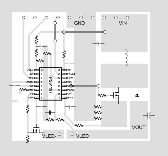
As for all switching power supplies, especially those providing high current and using high switching frequencies, layout is an important design step. If layout is not carefully done, the regulator could show instability as well as EMI problems. Therefore, use wide and short traces for high current paths. The VDD capacitor, C3 (see Figure 18) is the filter and noise decoupling capacitor for the internal linear regulator powering the internal circuitries. It must be placed as close as possible between the VDD and PGND pin to prevent any noise insertion to internal circuitry. The switch node at the drain of Q1 carries high current with fast rising and falling edges. Therefore, the connection between this node to the inductor and the Schottky diode must be kept as short and wide as possible. The ground of output capacitor EC2 must be kept close to input power ground or through a large ground plane because of the large ripple current returning to the input ground. When laying out signal grounds, TI recommends using short traces separate from power ground traces and connecting them together at a single point. Resistors R3, R4, and R7 (see Figure 18) are setting resistors for switching frequency and output overvoltage protection. To avoid unexpected noise coupling into the pins and affecting the accuracy, these resistors must be close to the pins with short and wide traces to AGND pin.
10.2 Layout Example
 Figure 23. TPS61197 Layout