SLVSAG8G September 2011 – June 2016 TPS61253 , TPS61254 , TPS61256 , TPS61258 , TPS61259 , TPS612592
UNLESS OTHERWISE NOTED, this document contains PRODUCTION DATA.
- 1 Features
- 2 Applications
- 3 Description
- 4 Revision History
- 5 Device Options
- 6 Pin Configuration and Functions
- 7 Specifications
- 8 Parameter Measurement Information
- 9 Detailed Description
- 10Application and Implementation
- 11Power Supply Recommendations
- 12Layout
- 13Device and Documentation Support
- 14Mechanical, Packaging, and Orderable Information
Package Options
Refer to the PDF data sheet for device specific package drawings
Mechanical Data (Package|Pins)
- YFF|9
Thermal pad, mechanical data (Package|Pins)
Orderable Information
12 Layout
12.1 Layout Guidelines
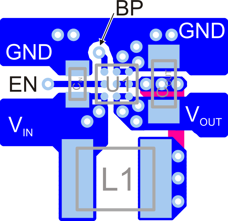
For all switching power supplies, the layout is an important step in the design, especially at high peak currents and high switching frequencies. If the layout is not carefully done, the regulator could show stability problems as well as EMI problems. Therefore, use wide and short traces for the main current path and for the power ground tracks. The input capacitor, output capacitor, and the inductor should be placed as close as possible to the IC. Use a common ground node for power ground and a different one for control ground to minimize the effects of ground noise. Connect these ground nodes at any place close to the ground pins of the IC.
12.2 Layout Example
 Figure 43. Suggested Layout (Top)
12.3 Thermal Considerations
Implementation of integrated circuits in low-profile and fine-pitch surface-mount packages typically requires special attention to power dissipation. Many system-dependent issues such as thermal coupling, airflow, added heat sinks and convection surfaces, and the presence of other heat-generating components affect the power-dissipation limits of a given component.
Three basic approaches for enhancing thermal performance are listed below:
- Improving the power dissipation capability of the PCB design
- Improving the thermal coupling of the component to the PCB
- Introducing airflow in the system
As power demand in portable designs is more and more important, designers must figure the best trade-off between efficiency, power dissipation and solution size. Due to integration and miniaturization, junction temperature can increase significantly which could lead to bad application behaviors (i.e. premature thermal shutdown or worst case reduce device reliability).
Junction-to-ambient thermal resistance is highly application and board-layout dependent. In applications where high maximum power dissipation exists (e.g. TPS61253 or TPS61259 based solutions), special care must be paid to thermal dissipation issues in board design. The device operating junction temperature (TJ) should be kept below 125°C.