SLVSAG8G September 2011 – June 2016 TPS61253 , TPS61254 , TPS61256 , TPS61258 , TPS61259 , TPS612592
UNLESS OTHERWISE NOTED, this document contains PRODUCTION DATA.
- 1 Features
- 2 Applications
- 3 Description
- 4 Revision History
- 5 Device Options
- 6 Pin Configuration and Functions
- 7 Specifications
- 8 Parameter Measurement Information
- 9 Detailed Description
- 10Application and Implementation
- 11Power Supply Recommendations
- 12Layout
- 13Device and Documentation Support
- 14Mechanical, Packaging, and Orderable Information
Package Options
Refer to the PDF data sheet for device specific package drawings
Mechanical Data (Package|Pins)
- YFF|9
Thermal pad, mechanical data (Package|Pins)
Orderable Information
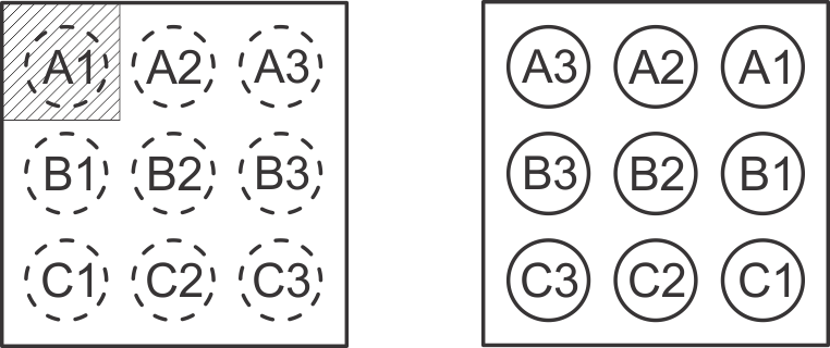
6 Pin Configuration and Functions

Pin Functions
| PIN | I/O | DESCRIPTION | |
|---|---|---|---|
| NAME | NO. | ||
| BP | C3 | I | This is the mode selection pin of the device and is only of relevance when the device is disabled (EN = Low). This pin must not be left floating and must be terminated. Refer to Table 2 for more details. |
| BP = Low: The device is in true shutdown mode. | |||
| BP = High: The output is biased at the input voltage level with a maximum load current capability of ca. 150mA. In standby mode, the device only consumes a standby current of 21µA (typ). | |||
| EN | B3 | I | This is the enable pin of the device. Connecting this pin to ground forces the device into shutdown mode. Pulling this pin high enables the device. This pin must not be left floating and must be terminated. |
| GND | C1, C2 | Ground pin. | |
| SW | B1, B2 | I/O | This is the switch pin of the converter and is connected to the drain of the internal Power MOSFETs. |
| VIN | A3 | I | Power supply input. |
| VOUT | A1, A2 | O | Boost converter output. |