SLVS957E June 2009 – April 2016 TPS61300 , TPS61301 , TPS61305
PRODUCTION DATA.
- 1 Features
- 2 Applications
- 3 Description
- 4 Revision History
- 5 Device Comparison Table
- 6 Pin Configuration and Functions
- 7 Specifications
-
8 Detailed Description
- 8.1 Overview
- 8.2 Functional Block Diagrams
- 8.3
Feature Description
- 8.3.1 Safety Timer Accuracy
- 8.3.2 LED Failure Modes and Overvoltage Protection
- 8.3.3 Start-Up Sequence
- 8.3.4 Power Good (Flash Ready)
- 8.3.5 LED Temperature Monitoring (TPS61305, TPS61305A, TPS61306)
- 8.3.6 Hot Die Detector
- 8.3.7 NRESET Input: Hardware Enable and Disable
- 8.3.8 ENDCL Input: DC Light Hardware Control
- 8.3.9 Flashlight Blanking (Tx-MASK)
- 8.3.10 Undervoltage Lockout
- 8.3.11 Storage Capacitor Active Cell Balancing
- 8.3.12 RED Light Privacy Indicator
- 8.3.13 White LED Privacy Indicator
- 8.3.14 Storage Capacitor, Precharge Voltage Calibration
- 8.3.15 Storage Capacitor, Adaptive Precharge Voltage
- 8.3.16 Serial Interface Description
- 8.4
Device Functional Modes
- 8.4.1 Down-Mode in Voltage Regulation Mode
- 8.4.2 LED High-Current Regulators, Unused Inputs
- 8.4.3 Power-Save Mode Operation, Efficiency
- 8.4.4 Mode of Operation: DC Light and Flashlight
- 8.4.5 Flash Strobe is Level Sensitive (STT = 0): LED Strobe Follows FLASH_SYNC Input
- 8.4.6 Flash Strobe Is Leading Edge Sensitive (STT = 1): One-Shot LED Strobe
- 8.4.7 Current Limit Operation
- 8.4.8 Hardware Voltage Mode Selection
- 8.4.9 Shutdown
- 8.4.10 Thermal Shutdown
- 8.4.11 F/S-Mode Protocol
- 8.4.12 HS-Mode Protocol
- 8.4.13 TPS6130xx I2C Update Sequence
- 8.5
Register Maps
- 8.5.1 Slave Address Byte
- 8.5.2 Register Address Byte
- 8.5.3 REGISTER1 (TPS61300, TPS61301)
- 8.5.4 REGISTER1 (TPS61305, TPS61305A, TPS61306)
- 8.5.5 REGISTER2 (TPS61300, TPS61301)
- 8.5.6 REGISTER2 (TPS61305, TPS61305A, TPS61306)
- 8.5.7 REGISTER3
- 8.5.8 REGISTER4
- 8.5.9 REGISTER5
- 8.5.10 REGISTER6 (TPS61300, TPS61301)
- 8.5.11 REGISTER6 (TPS61305, TPS61305A)
- 8.5.12 REGISTER7
-
9 Application and Implementation
- 9.1 Application Information
- 9.2 Typical Applications
- 9.3
System Examples
- 9.3.1 2x 600-mA High-Power White LED Solution Featuring Privacy Indicator
- 9.3.2 White LED Flashlight Driver and Audio Amplifier Power Supply Operating Simultaneously
- 9.3.3 White LED Flashlight Driver and Audio Amplifier Power Supply Operating Simultaneously
- 9.3.4 White LED Flashlight Driver and Audio Amplifier Power Supply Exclusive Operation
- 9.3.5 White LED Flashlight Driver and Auxiliary Lighting Zone Power Supply
- 9.3.6 TPS61300, Typical Application
- 9.3.7 TPS61301, Typical Application
- 9.3.8 TPS61305 Typical Application
- 9.3.9 TPS61306, Typical Application
- 10Power Supply Recommendations
- 11Layout
- 12Device and Documentation Support
- 13Mechanical, Packaging, and Orderable Information
Package Options
Mechanical Data (Package|Pins)
- YFF|20
Thermal pad, mechanical data (Package|Pins)
Orderable Information
9 Application and Implementation
NOTE
Information in the following applications sections is not part of the TI component specification, and TI does not warrant its accuracy or completeness. TI’s customers are responsible for determining suitability of components for their purposes. Customers should validate and test their design implementation to confirm system functionality.
9.1 Application Information
The TPS6130xx can drive up to three white LEDs in parallel (400-mA, 800-mA, and 400-mA maximum flash current). The extended high-current mode (HC_SEL) allows up to 1025-mA, 2050-mA, and 1025-mA flash current. The 2-MHz switching frequency allows the use of small and low profile passive components.
9.2 Typical Applications
9.2.1 4100-mA Two White High-Power LED Flashlight Featuring Storage Capacitor
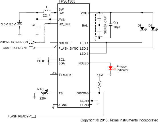 Figure 72. 4100-mA Two White High-Power LED Flashlight Featuring Storage Capacitor
9.2.1.1 Design Requirements
For this design example, use the parameters listed in Table 21 as the input parameters.
Table 21. TPS61305 Design Requirement
| DESIGN PARAMETER | EXAMPLE VALUE |
|---|---|
| Input Voltage Range | 2.5 V to 5.5 V |
| Output Voltage | 4.95 V |
| Operating Freqency | 2 MHz |
9.2.1.2 Detailed Design Procedure
9.2.1.2.1 Inductor Selection
A boost converter requires two main passive components for storing energy during the conversion. A boost inductor and a storage capacitor at the output are required. The TPS6130xx device integrates a current limit protection circuitry. The valley current of the PMOS rectifier is sensed to limit the maximum current flowing through the synchronous rectifier and the inductor. The valley peak current limit (250 mA, 500 mA, 1250 mA, or 1750 mA) is user selectable through the I2C interface.
To optimize solution size, the TPS6130xx device has been designed to operate with inductance values between a minimum of 1.3 μH and maximum of 2.9 μH. TI recommends a 2.2-μH inductance in typical high current white LED applications.
The highest peak current through the inductor and the power switch depends on the output load, the input and output voltages. Estimation of the maximum average inductor current and the maximum inductor peak current can be done using Equation 2 and Equation 3:


where
- f = switching frequency (2 MHz)
- L = inductance value (2.2 μH)
- η = estimated efficiency (85%)
The losses in the inductor caused by magnetic hysteresis losses and copper losses are a major parameter for total circuit efficiency.
9.2.1.2.2 Input Capacitor
TI recommends low ESR ceramic capacitors for good input voltage filtering. TI recommends a 10-μF input capacitor to improve transient behavior of the regulator and EMI behavior of the total power supply circuit. The input capacitor must be placed as close as possible to the input pin of the converter.
9.2.1.2.3 Output Capacitor
The major parameter necessary to define the output capacitor is the maximum allowed output voltage ripple of the converter. This ripple is determined by two parameters of the capacitor, the capacitance and the ESR. It is possible to calculate the minimum capacitance needed for the defined ripple, supposing that the ESR is zero, by using Equation 4:

where
- f is the switching frequency and ΔV is the maximum allowed ripple
With a chosen ripple voltage of 10 mV, a minimum capacitance of 10 μF is needed. The total ripple is larger due to the ESR of the output capacitor. This additional component of the ripple can be calculated using Equation 5:
The total ripple is the sum of the ripple caused by the capacitance and the ripple caused by the ESR of the capacitor. Additional ripple is caused by load transients. This means that the output capacitor has to completely supply the load during the charging phase of the inductor. A reasonable value of the output capacitance depends on the speed of the load transients and the load current during the load change.
For the standard current white LED application (HC_SEL = 0, TPS6130xx), a minimum of 3-μF effective output capacitance is usually required when operating with 2.2-μH (typical) inductors. For solution size reasons, this is usually one or more X5R or X7R ceramic capacitors.
Depending on the material, size and therefore margin to the rated voltage of the used output capacitor, degradation on the effective capacitance can be observed. This loss of capacitance is related to the DC bias voltage applied. TI recommends ensuring the selected capacitors are showing enough effective capacitance under real operating conditions.
To support high-current camera flash application (HC_SEL = 1), the converter is designed to work with a low voltage super-capacitor on the output to take advantage of the benefits they offer. A low-voltage super-capacitor in the 0.1-F to 1.5-F range, and with ESR larger than 40 mΩ, is suitable in the TPS6130xx application circuit. For this device the output capacitor must be connected between the VOUT pin and a good ground connection.
9.2.1.2.4 NTC Selection (TPS61305, TPS61305A, TPS61306)
The TPS61305, TPS61305A, and TPS61306 require a negative thermistor (NTC) for sensing the LED temperature. Once the temperature monitoring feature is activated, a regulated bias current (≈24 μA) will be driven out of the TS port and produce a voltage across the thermistor.
If the temperature of the NTC-thermistor rises due to the heat dissipated by the LED, the voltage on the TS input pin decreases. When this voltage goes below the warning threshold, the LEDWARN bit in REGISTER6 is set. This flag is cleared by reading the register.
If the voltage on the TS input decreases further and falls below hot threshold, the LEDHOT bit in REGISTER6 is set and the device goes automatically in shutdown mode to avoid damaging the LED. This status is latched until the LEDHOT flag gets cleared by software.
The selection of the NTC-thermistor value strongly depends on the power dissipated by the LED and all components surrounding the temperature sensor and on the cooling capabilities of each specific application. With a 220-kΩ (at 25°C) thermistor, the valid temperature window is set between 60°C to 90°C. The temperature window can be enlarged by adding external resistors to the TS pin application circuit. To ensure proper triggering of the LEDWARN and LEDHOT flags in noisy environments, the TS signal may require additional filtering capacitance.
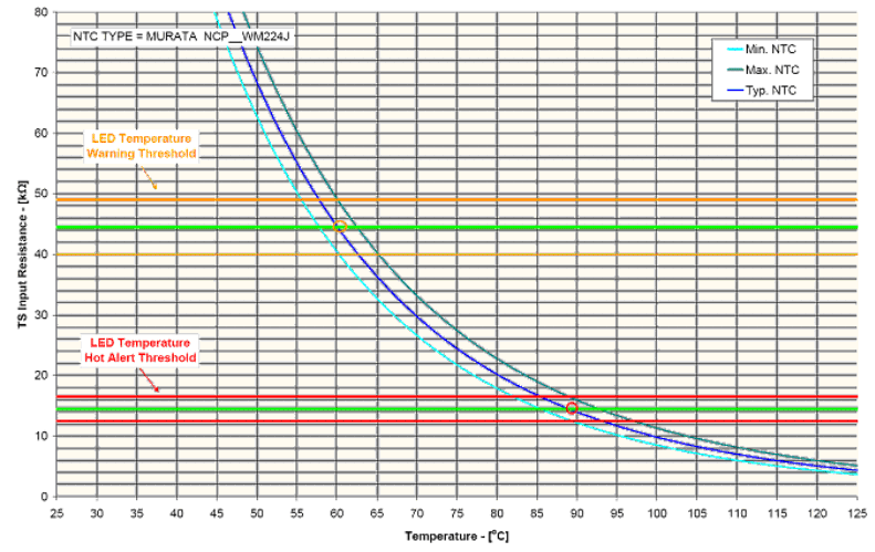 Figure 73. Temperature Monitoring Characteristic
9.2.1.2.5 Checking Loop Stability
The first step of circuit and stability evaluation is to look from a steady-state perspective at the following signals:
- Switching node, SW
- Inductor current, IL
- Output ripple voltage, VOUT(AC)
These are the basic signals that need to be measured when evaluating a switching converter. When the switching waveform shows large duty cycle jitter or the output voltage or inductor current shows oscillations the regulation loop may be unstable. This is often a result of improper board layout or L-C combination.
As a next step in the evaluation of the regulation loop the load transient response needs to be tested. VOUT can be monitored for settling time, overshoot or ringing that helps judge the converter's stability. Without any ringing, the loop has usually more than 45° of phase margin.
Because the damping factor of the circuitry is directly related to several resistive parameters, such as MOSFET rDS(on), that are temperature dependant, the loop stability analysis has to be done over the input voltage range, output current range, and temperature range.
9.2.1.3 Application Curves
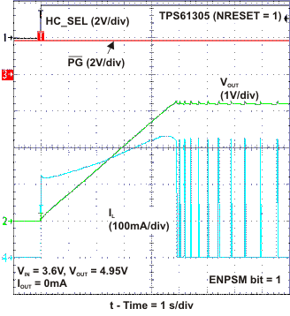 Figure 74. Storage Capacitor Precharge (HC_SEL = 1)
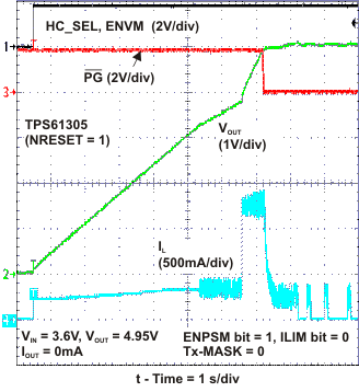 Figure 76. Storage Capacitor Charge-Up (HC_SEL = 1)
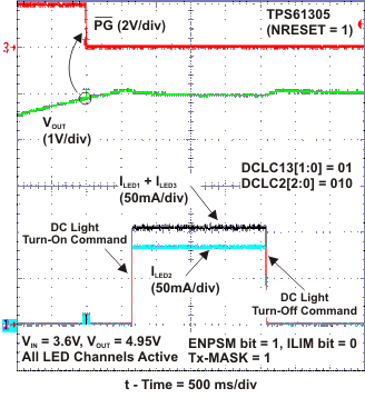 Figure 78. DC Light Operation (HC_SEL = 1)
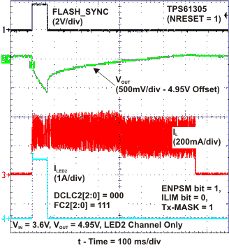 Figure 80. Flash Sequence (HC_SEL = 1)
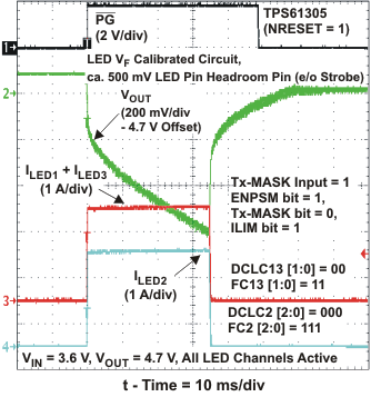 Figure 82. Flash Sequence (HC_SEL = 1)
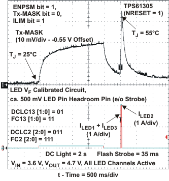 Figure 84. Junction Temperature Monitoring (HC_SEL = 1)
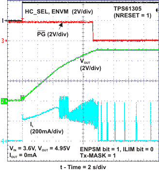 Figure 75. Storage Capacitor Charge-Up (HC_SEL = 1)
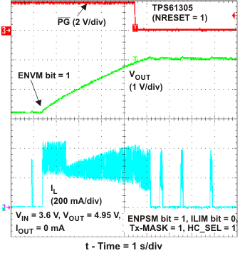 Figure 77. Storage Capacitor Charge-Up (HC_SEL = 1)
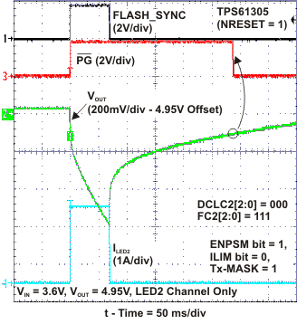 Figure 79. Flash Sequence (HC_SEL = 1)
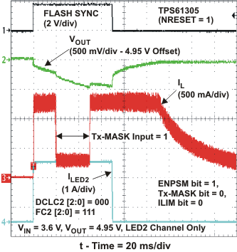 Figure 81. Flash Sequence (HC_SEL = 1)
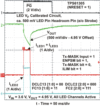 Figure 83. Flash Sequence (HC_SEL = 1)
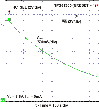 Figure 85. Shutdown (HC_SEL = 1)
9.2.2 TPS61300 Typical Application
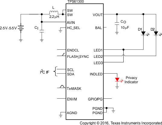 Figure 86. TPS61300 Typical Application Circuit
9.2.2.1 Design Requirement
For this design example, use the parameters listed in Table 22 as the input parameters.
Table 22. TPS61300 Design Requirement
| DESIGN PARAMETER | EXAMPLE VALUE |
|---|---|
| Input Voltage Range | 2.5 V to 5.5 V |
| Output Voltage | 4.95 V |
| Operating Freqency | 2 MHz |
9.2.2.2 Application Curves
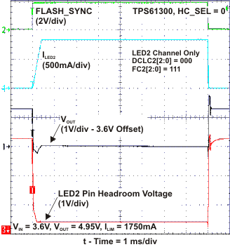 Figure 87. Flash Sequence (HC_SEL = 0)
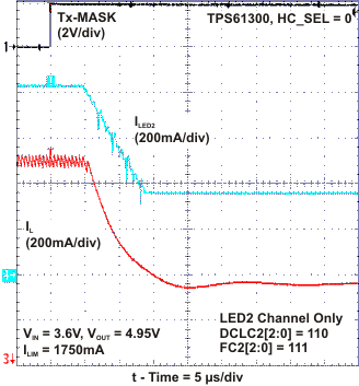 Figure 89. Tx-Masking Operation (HC_SEL = 0)
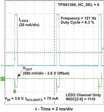 Figure 91. Low-Light Dimming Mode Operation
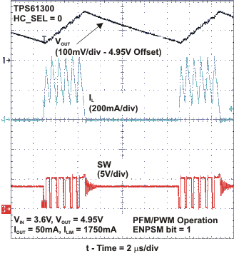 Figure 93. PFM Operation
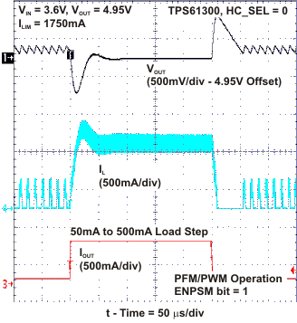 Figure 95. Voltage Mode Load Transient Response
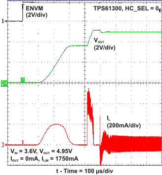 Figure 97. Start-Up Into Voltage Mode Operation
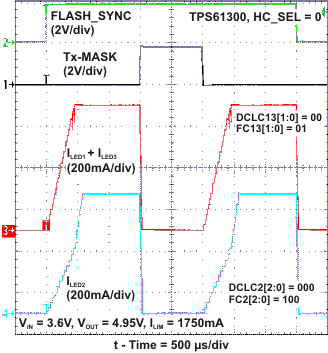 Figure 88. Tx-Masking Operation (HC_SEL = 0)
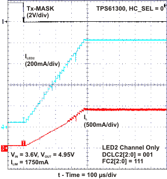 Figure 90. Tx-Masking Operation (HC_SEL = 0)
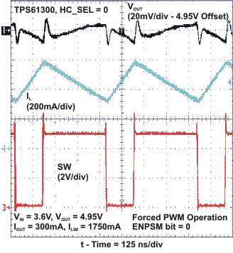 Figure 92. PWM Operation
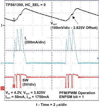 Figure 94. Down-Mode Operation (Voltage Mode)
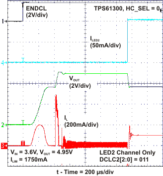 Figure 96. Start-Up Into DC Light Operation
9.3 System Examples
9.3.1 2x 600-mA High-Power White LED Solution Featuring Privacy Indicator
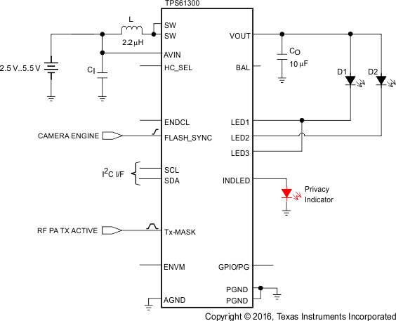 Figure 98. 2× 600-mA High-Power White LED Solution Featuring Privacy Indicator
9.3.2 White LED Flashlight Driver and Audio Amplifier Power Supply Operating Simultaneously
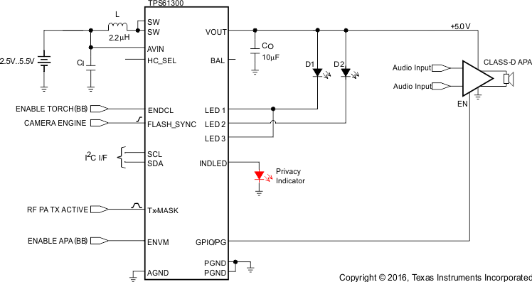 Figure 99. White LED Flashlight Driver and Audio Amplifier Power Supply Operating Simultaneously
9.3.3 White LED Flashlight Driver and Audio Amplifier Power Supply Operating Simultaneously
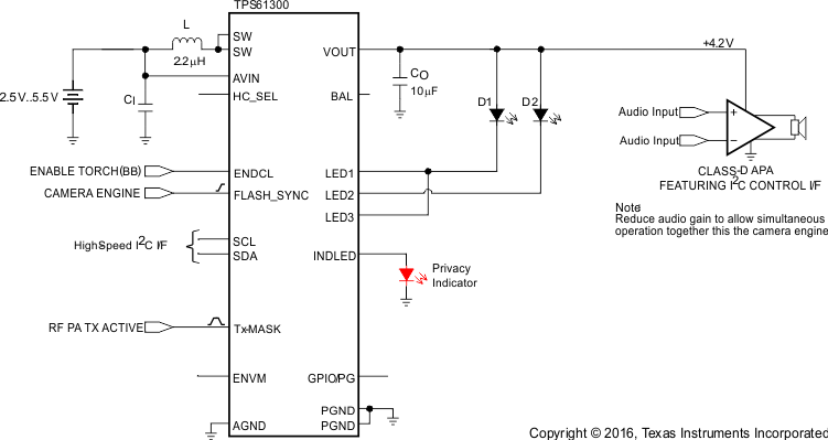 Figure 100. White LED Flashlight Driver and Audio Amplifier Power Supply Operating Simultaneously
9.3.4 White LED Flashlight Driver and Audio Amplifier Power Supply Exclusive Operation
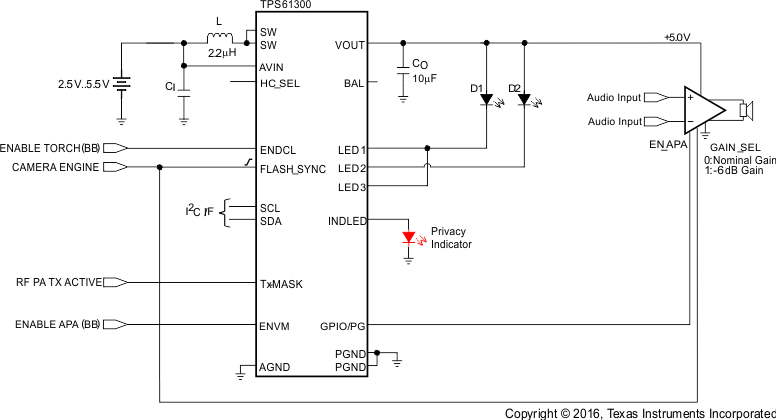 Figure 101. White LED Flashlight Driver and Audio Amplifier Power Supply Exclusive Operation
9.3.5 White LED Flashlight Driver and Auxiliary Lighting Zone Power Supply
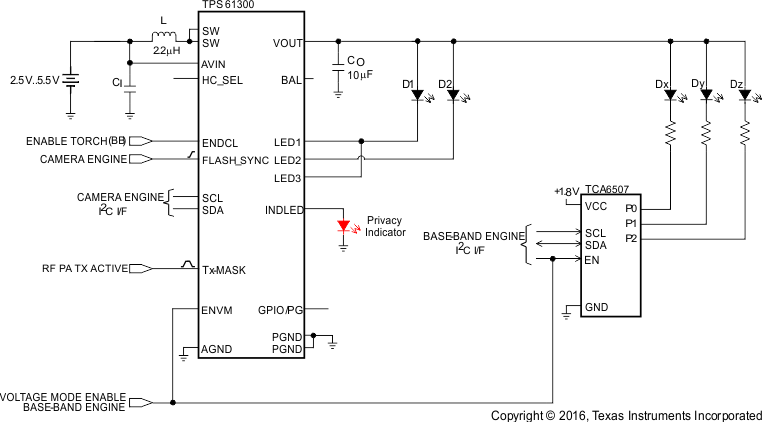 Figure 102. White LED Flashlight Driver and Auxiliary Lighting Zone Power Supply
9.3.6 TPS61300, Typical Application
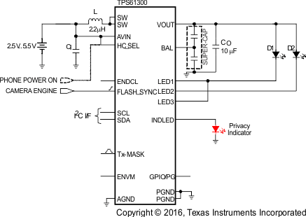 Figure 103. TPS61300, Typical Application
9.3.7 TPS61301, Typical Application
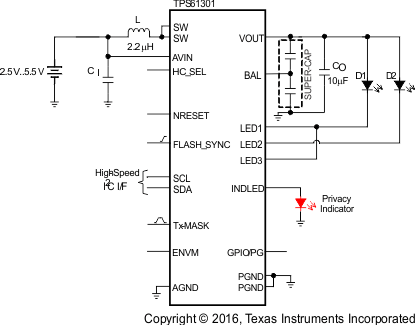 Figure 104. TPS61301, Typical Application
9.3.8 TPS61305 Typical Application
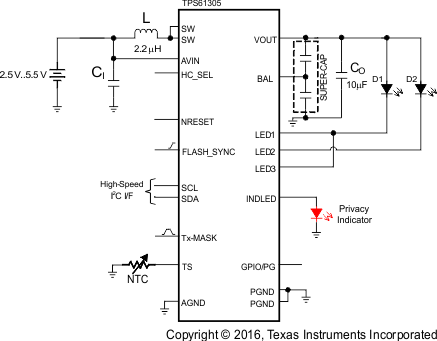 Figure 105. TPS61305, Typical Application
9.3.9 TPS61306, Typical Application
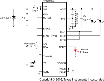 Figure 106. TPS61306, Typical Application