SLVSAM2E November 2011 – May 2017 TPS62160 , TPS62161 , TPS62162 , TPS62163
PRODUCTION DATA.
- 1 Features
- 2 Applications
- 3 Description
- 4 Revision History
- 5 Device Voltage Options
- 6 Pin Configuration and Functions
- 7 Specifications
- 8 Detailed Description
- 9 Application and Implementation
- 10Power Supply Recommendations
- 11Layout
- 12Device and Documentation Support
- 13Mechanical, Packaging, and Orderable Information
Package Options
Mechanical Data (Package|Pins)
- DSG|8
Thermal pad, mechanical data (Package|Pins)
- DSG|8
Orderable Information
11 Layout
11.1 Layout Guidelines
A proper layout is critical for the operation of a switched mode power supply, even more at high switching frequencies. Therefore the PCB layout of the TPS6216x demands careful attention to ensure operation and to get the performance specified. A poor layout can lead to issues like poor regulation (both line and load), stability and accuracy weaknesses, increased EMI radiation, and noise sensitivity.
Provide low inductive and resistive paths to ground for loops with high di/dt. Therefore paths conducting the switched load current should be as short and wide as possible. Provide low capacitive paths, with respect to all other nodes, for wires with high dv/dt. Therefore the input and output capacitance should be placed as close as possible to the IC pins and parallel wiring over long distances as well as narrow traces should be avoided. Loops which conduct an alternating current should outline an area as small as possible, as this area is proportional to the energy radiated.
Also sensitive nodes like FB and VOS should be connected with short wires, not nearby high dv/dt signals, such as SW. As they carry information about the output voltage, they should be connected as close as possible to the actual output voltage (at the output capacitor). Signals not assigned to power transmission, such as the feedback divider, should refer to the signal ground (AGND) and always be separated from the power ground (PGND).
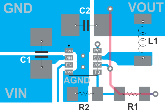
In summary, the input capacitor should be placed as close as possible to the VIN and PGND pin of the IC. This connections should be done with wide and short traces. The output capacitor should be placed such that its ground is as close as possible to the IC's PGND pins - avoiding additional voltage drop in traces. This connection should also be made short and wide. The inductor should be placed close to the SW pin and connect directly to the output capacitor - minimizing the loop area between the SW pin, inductor, output capacitor and PGND pin. The feedback resistors, R1 and R2, should be placed close to the IC and connect directly to the AGND and FB pins. Those connections (including VOUT) to the resistors and especially to the VOS pin should stay away from noise sources, such as the inductor. The VOS pin should connect in the shortest way to VOUT at the output capacitor, while the VOUT connection to the feedback divider can connect at the load.
A single point grounding scheme should be implemented with all grounds (AGND, PGND and the thermal pad) connecting at the IC's exposed thermal pad. See Figure 42 for the recommended layout of the TPS6216x. More detailed information can be found in the EVM Users Guide, SLVU483.
The exposed thermal pad must be soldered to the circuit board for mechanical reliability and to achieve appropriate power dissipation. Although the exposed thermal pad can be connected to a floating circuit board trace, the device has better thermal performance if it is connected to a larger ground plane. The exposed thermal pad is electrically connected to AGND.
11.2 Layout Example
 Figure 42. TPS6216x Board Layout
11.3 Thermal Considerations
Implementation of integrated circuits in low-profile and fine-pitch surface-mount packages typically requires special attention to power dissipation. Many system-dependent issues such as thermal coupling, airflow, added heat sinks and convection surfaces, and the presence of other heat-generating components affect the power-dissipation limits of a given component.
Three basic approaches for enhancing thermal performance are listed below:
- Improving the power dissipation capability of the PCB design
- Improving the thermal coupling of the component to the PCB by soldering the exposed thermal pad
- Introducing airflow in the system
For more details on how to use the thermal parameters, see the application reports Thermal Characteristics of Linear and Logic Packages Using JEDEC PCB Designs, SZZA017 and Semiconductor and IC Package Thermal Metrics, SPRA953.
The TPS6216x is designed for a maximum operating junction temperature (TJ) of 125°C. Therefore the maximum output power is limited by the power losses that can be dissipated over the actual thermal resistance, given by the package and the surrounding PCB structures. If the thermal resistance of the package is given, the size of the surrounding copper area and a proper thermal connection of the IC can reduce the thermal resistance. To get an improved thermal behavior, TI recommends to use top layer metal to connect the device with wide and thick metal lines. Internal ground layers can connect to vias directly under the IC for improved thermal performance.
If short circuit or overload conditions are present, the device is protected by limiting internal power dissipation.