SLVS681F June 2006 – August 2014 TPS62400 , TPS62401 , TPS62402 , TPS62403 , TPS62404
PRODUCTION DATA.
- 1 Features
- 2 Applications
- 3 Description
- 4 Revision History
- 5 Device Options
- 6 Pin Configuration and Functions
- 7 Specifications
- 8 Detailed Description
-
9 Application and Implementation
- 9.1 Application Information
- 9.2
Typical Applications
- 9.2.1
TPS6240x, Dual Outputs Step Down Converter
- 9.2.1.1 Design Requirements
- 9.2.1.2
Detailed Design Procedure
- 9.2.1.2.1 Converter1 Adjustable Default Output Voltage Setting: TPS62400
- 9.2.1.2.2 Converter1 Fixed Default Output Voltage Setting (TPS62401, TPS62402, TPS62403, TPS62404).
- 9.2.1.2.3 Converter 2 Adjustable Default Output Voltage Setting TPS62400:
- 9.2.1.2.4 Converter 2 Fixed Default Output Voltage Setting
- 9.2.1.2.5 Output Filter Design (Inductor and Output Capacitor)
- 9.2.1.3 Application Curves
- 9.2.2 Various Output Voltages
- 9.2.3 Dynamic Voltage Scaling on Converter 1 by DEF_1 Pin
- 9.2.1
TPS6240x, Dual Outputs Step Down Converter
- 10Power Supply Recommendations
- 11Layout
- 12Device and Documentation Support
- 13Mechanical, Packaging, and Orderable Information
Package Options
Mechanical Data (Package|Pins)
- DRC|10
Thermal pad, mechanical data (Package|Pins)
- DRC|10
Orderable Information
9 Application and Implementation
9.1 Application Information
The TPS6240x family of devices are synchronous dual step-down DC-DC converters. The devices provide two independent output voltage rails. The following information gives guidance on choosing external components to complete the application design.
9.2 Typical Applications
9.2.1 TPS6240x, Dual Outputs Step Down Converter
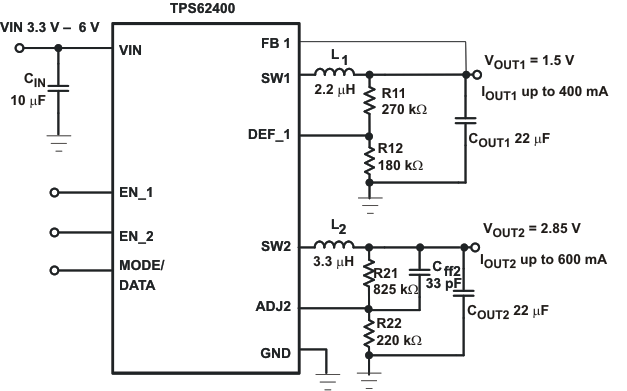 Figure 14. Typical Application Circuit 1.5V/2.85V Adjustable Outputs, Low PFM Voltage Ripple Optimized
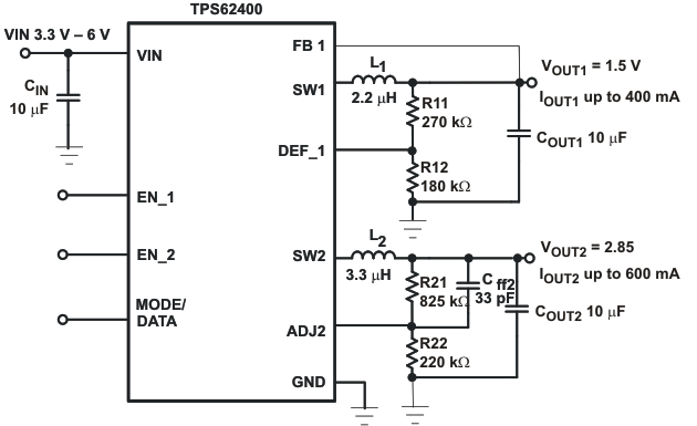 Figure 15. Typical Application Circuit 1.5V/2.85V Adjustable Outputs
9.2.1.1 Design Requirements
The step-down converter design can be adapted to different output voltage and load current needs by choosing external components appropriate. The following design procedure is adequate for whole VIN, VOUT and load current range of TPS6240x.
9.2.1.2 Detailed Design Procedure
9.2.1.2.1 Converter1 Adjustable Default Output Voltage Setting: TPS62400
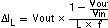
The output voltage can be calculated to:

To keep the operating current to a minimum, it is recommended to select R12 within a range of 180kΩ to 360kΩ. The sum of R12 and R11 should not exceed ~1MΩ. For higher output voltages than 3.3V, it is recommended to choose lower values than 180kΩ for R12. Route the DEF_1 line away from noise sources, such as the inductor or the SW1 line. The FB1 line needs to be directly connected to the output capacitor. A feed-forward capacitor is not necessary.
9.2.1.2.2 Converter1 Fixed Default Output Voltage Setting (TPS62401, TPS62402, TPS62403, TPS62404).
The output voltage VOUT1 is selected with DEF_1 pin.
Pin DEF_1 = low:
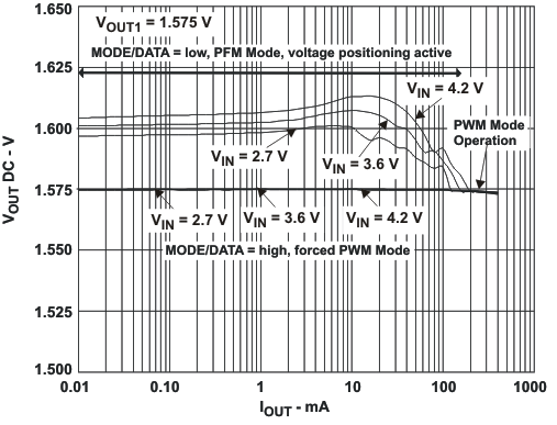
TPS62401, TPS62403 = 1.575V
Pin DEF_1 = high:
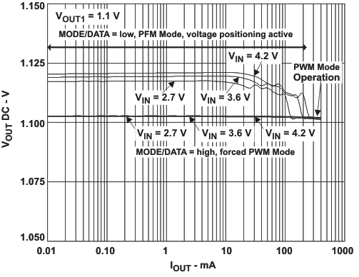
TS62401, TPS62403 = 1.1V
T62402: = 1.8V
T62404: = 1.9V
9.2.1.2.3 Converter 2 Adjustable Default Output Voltage Setting TPS62400:
The output voltage of converter 2 can be set by an external resistor network. For converter 2 the same recommendations apply as for converter1. In addition to that, a 33pF feed-forward Capacitor Cff2 for good load transient response should be used. The output voltage can be calculated to:

9.2.1.2.4 Converter 2 Fixed Default Output Voltage Setting
ADJ2 pin must be directly connected with VOUT2
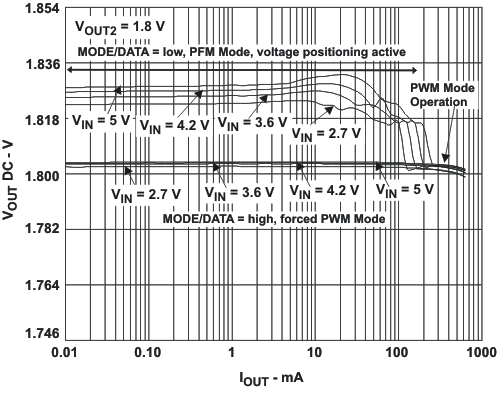
TPS62401, VOUT2 default = 1.8V
TPS62403, VOUT2 default = 2.8V
TPS62402, TPS62404, VOUT2 default = 3.3V
9.2.1.2.5 Output Filter Design (Inductor and Output Capacitor)
The converters are designed to operate with a minimum inductance of 1.75μH and minimum capacitance of 6μF. The device is optimized to operate with inductors of 2.2μH to 4.7μH and output capacitors of 10μF to 22μF.
9.2.1.2.5.1 Inductor Selection
The selected inductor has to be rated for its DC resistance and saturation current. The DC resistance of the inductor will influence directly the efficiency of the converter. Therefore an inductor with lowest DC resistance should be selected for highest efficiency.
Equation 6 calculates the maximum inductor current under static load conditions. The saturation current of the inductor should be rated higher than the maximum inductor current as calculated with Equation 7. This is recommended because during heavy load transient the inductor current rises above the calculated value.
with:
f = Switching Frequency (2.25MHz typical)
L = Inductor Value
ΔIL = Peak-to-Peak inductor ripple current
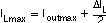
ILmax = Maximum Inductor current
The highest inductor current occurs at maximum Vin.
Open core inductors have a soft saturation characteristic and they can usually handle higher inductor currents versus a comparable shielded inductor.
A more conservative approach is to select the inductor current rating just for the maximum switch current of the corresponding converter. Take into consideration that the core material from inductor to inductor differs and this difference has an impact on the efficiency.
Refer to Table 7 and the typical application circuit examples for possible inductors.
Table 7. List of Inductors
| DIMENSIONS [mm3] | INDUCTOR TYPE | SUPPLIER |
|---|---|---|
| 3.2×2.6×1.0 | MIPW3226 | FDK |
| 3×3×0.9 | LPS3010 | Coilcraft |
| 2.8×2.6×1.0 | VLF3010 | TDK |
| 2.8x2.6×1.4 | VLF3014 | TDK |
| 3×3×1.4 | LPS3015 | Coilcraft |
| 3.9×3.9×1.7 | LPS4018 | Coilcraft |
9.2.1.2.5.2 Output Capacitor Selection
The advanced fast response voltage mode control scheme of the converters allows the use of tiny ceramic capacitors with a typical value of 10μF to 22μF, without having large output voltage under and overshoots during heavy load transients. Ceramic capacitors with low ESR values results in lowest output voltage ripple, and are therefore recommended. The output capacitor requires either X7R or X5R dielectric. Y5V and Z5U dielectric capacitors are not recommended due to their wide variation in capacitance.
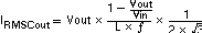
If ceramic output capacitors are used, the capacitor RMS ripple current rating always meets the application requirements. The RMS ripple current is calculated as:
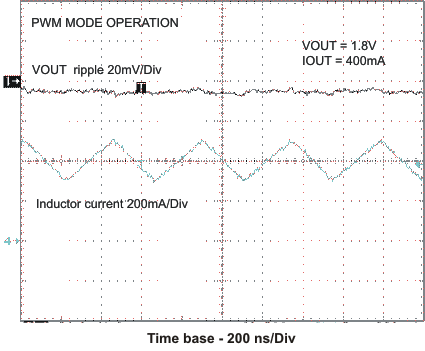
At nominal load current the inductive converters operate in PWM mode and the overall output voltage ripple is the sum of the voltage spike caused by the output capacitor ESR, plus the voltage ripple caused by charging and discharging the output capacitor:
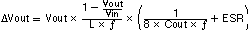
Where the highest output voltage ripple occurs at the highest input voltage Vin.
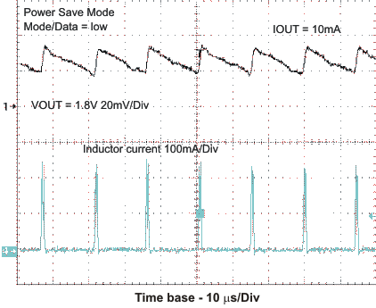
At light load currents the converters operate in Power Save Mode and the output voltage ripple is dependent on the output capacitor value. The output voltage ripple is set by the internal comparator delay and the external capacitor. Higher output capacitors like 22μF values minimize the voltage ripple in PFM Mode and tighten DC output accuracy in PFM Mode.
9.2.1.2.5.3 Input Capacitor Selection
Because of the nature of the buck converter having a pulsating input current, a low ESR input capacitor is required to prevent large voltage transients that can cause misbehavior of the device or interference with other circuits in the system. An input capacitor of 10μF is sufficient.
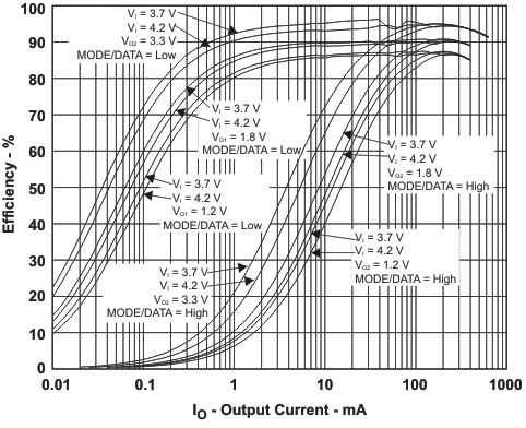
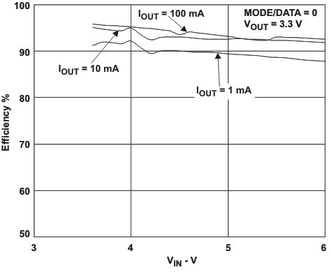
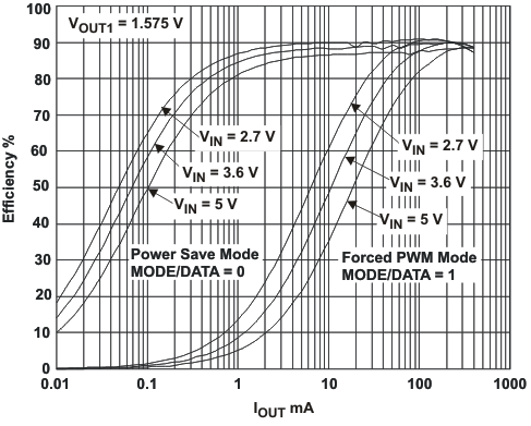
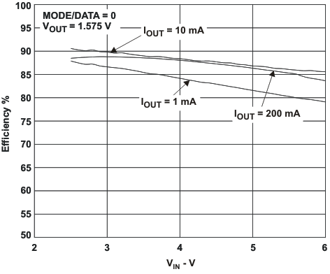
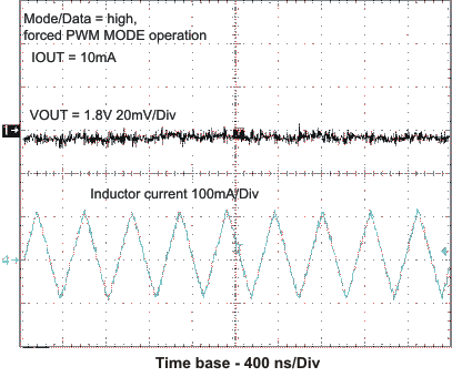
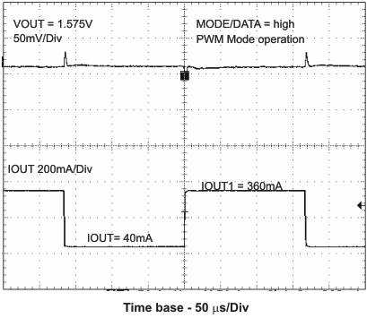
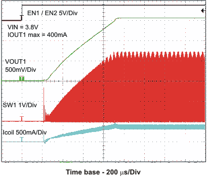
9.2.1.3 Application Curves
VIN = 3.6 V, and TA = 25 °C, unless otherwise noted.
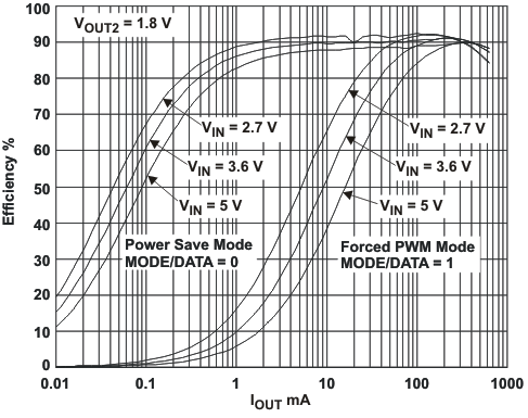
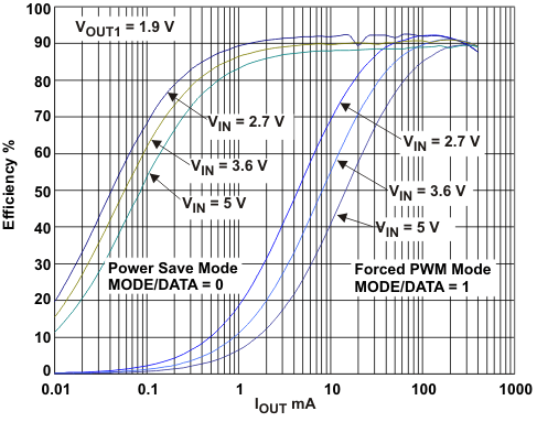
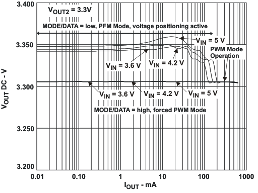
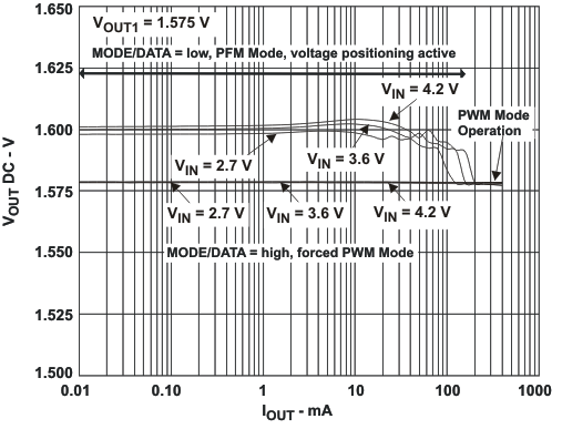
L = 2.2μH, COUT = 22μF
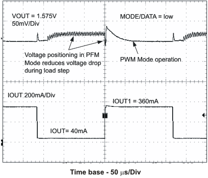
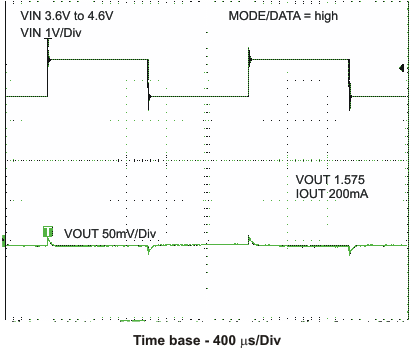
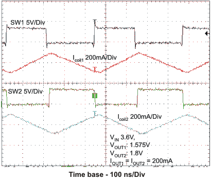
VOUT1 = 1.575V, VOUT2 = 1.8V
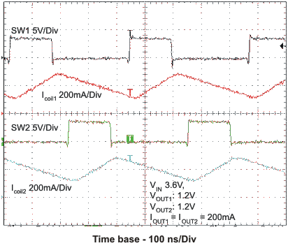
VOUT1 = 1.2V, VOUT2 = 1.2V
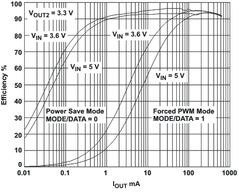
L = 3.3μH, COUT = 10μF
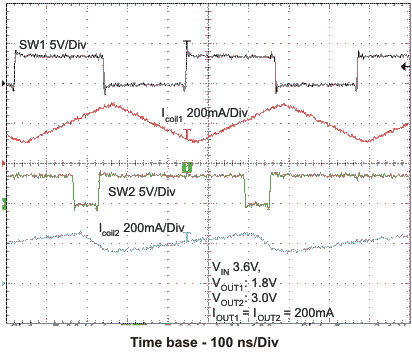
VOUT1 = 1.8V, VOUT2 = 3.0V
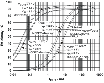
9.2.2 Various Output Voltages
The TPS6240x is able to be set for different output voltages. Some examples are shown below.
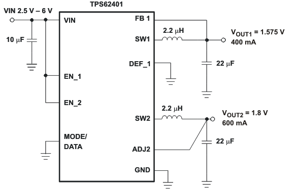 Figure 42. TPS62401 Fixed 1.575V/1.8V Outputs, Low PFM Voltage Ripple Optimized
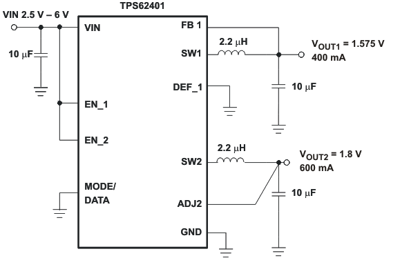 Figure 43. TPS62401 Fixed 1.575V/1.8V Outputs
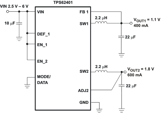 Figure 44. TPS62401 Fixed 1.1V/1.8V Outputs, Low PFM Ripple Voltage Optimized
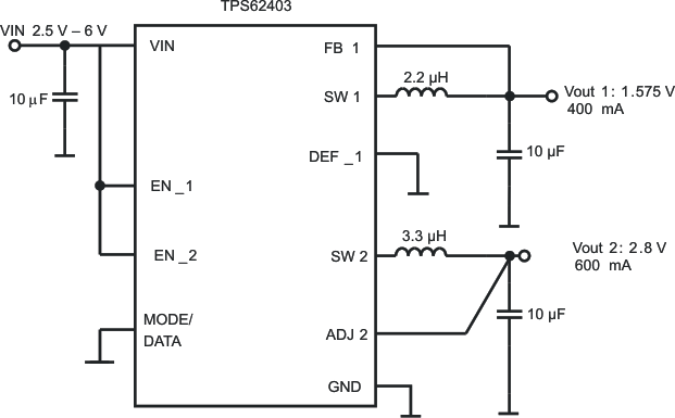 Figure 45. TPS62403 1.575V/2.8V Outputs
9.2.2.1 Design Requirements
The TPS6240x step-down converter is set to different output voltages.
9.2.2.2 Detailed Design Procedure
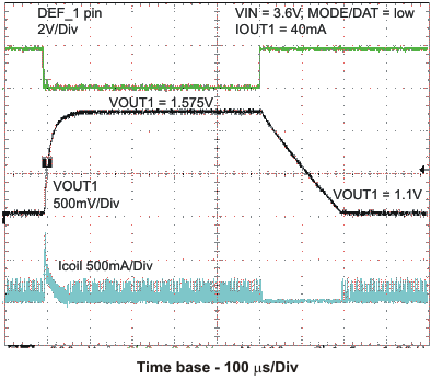
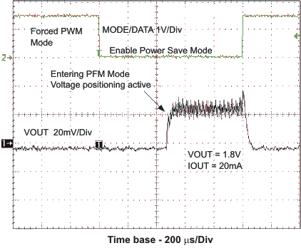
9.2.3 Dynamic Voltage Scaling on Converter 1 by DEF_1 Pin
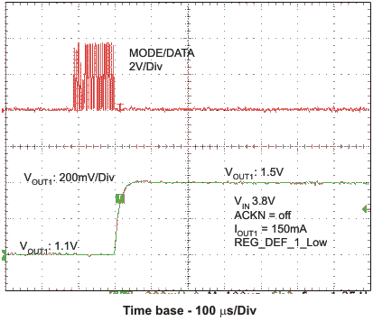
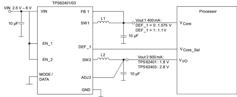 Figure 46. Dynamic Voltage Scaling on Converter 1 by DEF_1 Pin
9.2.3.1 Design Requirements
Control the output voltage of the converter 1 through DEF_1 pin by an external processor.
9.2.3.2 Detailed Design Procedure
Connect the DEF_1 pin to the VCore_Sel pin of an external processor, as shown in Figure 46. The processor determines the logic status of the DEF_1 pin which sets the output voltage of the converter 1.
Application Curves