SLUSDN9B November 2021 – July 2022 TPS62441-Q1 , TPS62442-Q1
PRODUCTION DATA
- 1 Features
- 2 Applications
- 3 Description
- 4 Revision History
- 5 Device Comparison Table
- 6 Pin Configuration and Functions
- 7 Specifications
- 8 Parameter Measurement Information
- 9 Detailed Description
- 10Application and Implementation
- 11Power Supply Recommendations
- 12Layout
- 13Device and Documentation Support
- 14Mechanical, Packaging, and Orderable Information
Package Options
Mechanical Data (Package|Pins)
- RQR|14
Thermal pad, mechanical data (Package|Pins)
- RQR|14
Orderable Information
10.1.2.1 Inductor Selection
The TPS6244x-Q1 is designed for a nominal 0.47-µH inductor with a switching frequency of typically 2.25 MHz. Larger values can be used to achieve a lower inductor current ripple but they can have a negative impact on efficiency and transient response. Smaller values than 0.47 µH cause a larger inductor current ripple, which causes larger negative inductor current in forced PWM mode at low or no output current. For a higher or lower nominal switching frequency, the inductance must be changed accordingly.
The inductor selection is affected by several effects like the following:
- Inductor ripple current
- Output ripple voltage
- PWM-to-PFM transition point
- Efficiency
In addition, the inductor selected has to be rated for appropriate saturation current and DC resistance (DCR). Equation 7 calculates the maximum inductor current.
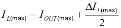
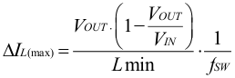
where
- IL(max) is the maximum inductor current.
- ΔIL(max) is the peak-to-peak inductor ripple current.
- Lmin is the minimum inductance at the operating point.
| Type | Inductance [µH] | Current [A](1) | For Device | Nominal Switching Frequency | Dimensions [L × B × H] mm |
Manufacturer(2) |
|---|---|---|---|---|---|---|
| XEL3520-801ME | 0.80 µH, ±20% | 2.0 | TPS62441-Q1 | 2.25 MHz | 3.5 × 3.2 × 2.0 | Coilcraft |
| XEL3520-561ME | 0.56 µH, ±20% | 2.4 | TPS62441-Q1 | 2.25 MHz | 3.5 × 3.2 × 2.0 | Coilcraft |
| XEL3515-561ME | 0.56 µH, ±20% | 4.5 | TPS62442-Q1 | 2.25 MHz | 3.5 × 3.2 × 1.5 | Coilcraft |
| XFL3012-681ME | 0.68 µH, ±20% | 2.1 | TPS62441-Q1 | 2.25 MHz | 3.0 × 3.0 × 1.2 | Coilcraft |
| XPL2010-681ML | 0.68 µH, ±20% | 1.5 | TPS62441-Q1 | 2.25 MHz | 2 × 1.9 × 1 | Coilcraft |
| DFE252012PD-R68M | 0.68 µH, ±20% | see data sheet | TPS62442-Q1 | 2.25 MHz | 2.5 × 2 × 1.2 | Murata |
| DFE252012PD-R47M | 0.47 µH, ±20% | see data sheet | TPS62442-Q1 | 2.25 MHz | 2.5 × 2 × 1.2 | Murata |
| DFE201612PD-R68M | 0.68 µH, ±20% | see data sheet | TPS62441-Q1 | 2.25 MHz | 2 × 1.6 × 1.2 | Murata |
| DFE201612PD-R47M | 0.47 µH, ±20% | see data sheet | TPS62442-Q1 | 2.25 MHz | 2 × 1.6 × 1.2 | Murata |
Calculating the maximum inductor current using the actual operating conditions gives the minimum saturation current of the inductor needed. TI recommends adding a margin of approximately 20%. A larger inductor value is also useful to get lower ripple current, but increases the transient response time and size as well.