SLUSEQ8A november   2021  – may 2023 TPS62441 , TPS62442

PRODUCTION DATA  

  1.   1
  2. Features
  3. Applications
  4. Description
  5. Revision History
  6. Device Comparison Table
  7. Pin Configuration and Functions
  8. Specifications
    1. 7.1 Absolute Maximum Ratings
    2. 7.2 ESD Ratings
    3. 7.3 Recommended Operating Conditions
    4. 7.4 Thermal Information
    5. 7.5 Electrical Characteristics
    6. 7.6 Timing Requirements
    7. 7.7 Typical Characteristics
  9. Parameter Measurement Information
    1. 8.1 Schematic
  10. Detailed Description
    1. 9.1 Overview
    2. 9.2 Functional Block Diagram
    3. 9.3 Feature Description
      1. 9.3.1 Precise Enable (EN)
      2. 9.3.2 COMP/FSET
      3. 9.3.3 MODE/SYNC
      4. 9.3.4 Undervoltage Lockout (UVLO)
      5. 9.3.5 Power-Good Output (PG)
      6. 9.3.6 Thermal Shutdown
    4. 9.4 Device Functional Modes
      1. 9.4.1 Pulse Width Modulation (PWM) Operation
      2. 9.4.2 Power Save Mode Operation (PWM/PFM)
      3. 9.4.3 100% Duty-Cycle Operation
      4. 9.4.4 Current Limit and Short-Circuit Protection
      5. 9.4.5 Output Discharge
      6. 9.4.6 Soft Start
  11. 10Application and Implementation
    1. 10.1 Application Information
      1. 10.1.1 Programming the Output Voltage
      2. 10.1.2 External Component Selection
        1. 10.1.2.1 Inductor Selection
        2. 10.1.2.2 Capacitor Selection
          1. 10.1.2.2.1 Input Capacitor
          2. 10.1.2.2.2 Output Capacitor
    2. 10.2 Typical Application
      1. 10.2.1 Design Requirements
      2. 10.2.2 Detailed Design Procedure
      3. 10.2.3 Application Curves
    3. 10.3 Power Supply Recommendations
    4. 10.4 Layout
      1. 10.4.1 Layout Guidelines
      2. 10.4.2 Layout Example
  12. 11Device and Documentation Support
    1. 11.1 Device Support
      1. 11.1.1 Third-Party Products Disclaimer
    2. 11.2 Documentation Support
      1. 11.2.1 Related Documentation
    3. 11.3 Receiving Notification of Documentation Updates
    4. 11.4 Support Resources
    5. 11.5 Trademarks
    6. 11.6 Electrostatic Discharge Caution
    7. 11.7 Glossary
  13. 12Mechanical, Packaging, and Orderable Information

Package Options

Mechanical Data (Package|Pins)
Thermal pad, mechanical data (Package|Pins)
Orderable Information

Description

The TPS6244x is a family of pin-to-pin dual 1-A, dual 2-A, and 3-A/1-A high-efficiency and easy-to-use synchronous step-down DC/DC converters. The device family is based on a peak current mode control topology. The devices are designed for industrial applications such as motor drives and robotics. Low resistive switches allow up to 3-A continuous output current and total maximum output current up to 4-A at high ambient temperature. The switching frequency is externally adjustable from 1.8 MHz to 4 MHz and can also be synchronized to an external clock in the same frequency range. In PWM/PFM mode, the TPS6244x automatically enters power save mode at light loads to maintain high efficiency across the whole load range. The TPS6244x provides a 1% output voltage accuracy in PWM mode, which helps design a power supply with high output voltage accuracy.

The TPS6244x is available as an adjustable voltage version, packaged in a VQFN package.

Package Information
PART NUMBER PACKAGE(1)BODY SIZE (NOM)
TPS62441RQR (VQFN, 14)2.30 mm × 2.70 mm
TPS62442
For all available packages, see the orderable addendum at the end of the data sheet.
GUID-20211117-SS0I-KF1J-PXP7-HDV8KSB1KQWH-low.svgSchematic
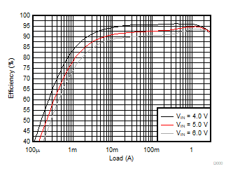
GUID-0D3B1E11-BA10-4328-A166-BA0F0C3C4DCE-low.gifEfficiency Versus Output Current; VOUT = 3.3 V, PWM/PFM, fsw = 2.25 MHz