SLVSCL9A February 2016 – February 2016 TPS62480
PRODUCTION DATA.
- 1 Features
- 2 Applications
- 3 Description
- 4 Revision History
- 5 Pin Configuration and Functions
- 6 Specifications
- 7 Detailed Description
- 8 Application and Implementation
- 9 Power Supply Recommendations
- 10Layout
- 11Device and Documentation Support
- 12Mechanical, Packaging, and Orderable Information
Package Options
Mechanical Data (Package|Pins)
- RNC|16
Thermal pad, mechanical data (Package|Pins)
Orderable Information
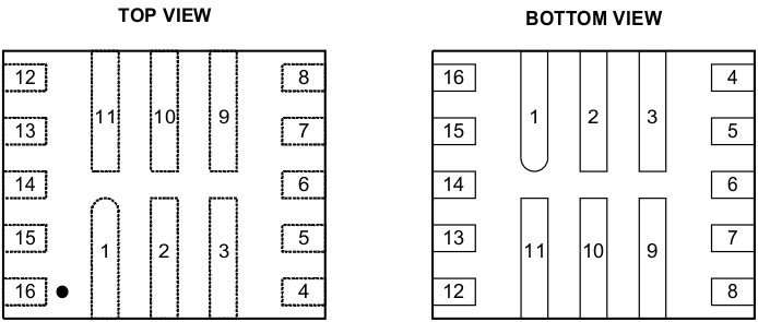
5 Pin Configuration and Functions
RNC Package
16-Pin (VQFN)

space
space
Pin Functions
| PIN | I/O | DESCRIPTION | |
|---|---|---|---|
| NAME | NO. | ||
| PGND1 | 1 | Power Ground Phase 1 (master) | |
| SW1 | 2 | Switch Node Phase 1 (master) , connected to the internal MOSFET switches | |
| VIN1 | 3 | Supply voltage Phase 1 (master) | |
| EN | 4 | I | Enable input (High=Enabled, Low = Disabled) |
| PG | 5 | O | Power Good (open drain, requires pull-up resistor) |
| VSEL | 6 | I | Output Voltage Select (High = VOUT2, Low=VOUT1) , VOUT1 < VOUT2 |
| TG | 7 | O | Thermal Good (open drain, requires pull-up resistor) |
| MODE | 8 | I | Operating mode selection (Low=Automatic PWM/PSM, High = Forced PWM) |
| VIN2 | 9 | Supply voltage Phase 2 | |
| SW2 | 10 | Switch node Phase 2, connected to the internal MOSFET switches | |
| PGND2 | 11 | Power Ground Phase 2 | |
| SS/TR | 12 | O | Soft-Start / Tracking. An external capacitor connected to this pin sets the output voltage rise time. |
| AGND | 13 | Analog Ground | |
| FB | 14 | Output voltage feedback for the adjustable version. Connect resistive voltage divider to this pin. | |
| RS | 15 | Resistor Select. Connect resistor that sets the level for the second output voltage here (activated by VSEL= High) | |
| VO | 16 | VOUT detection (connect to VOUT, output discharge is internally connected to this pin) | |