SLVSFS3B September   2020  – July 2021 TPS62868 , TPS62869

PRODUCTION DATA  

  1. Features
  2. Applications
  3. Description
  4. Revision History
  5. Device Options
  6. Pin Configuration and Functions
  7. Specifications
    1. 7.1 Absolute Maximum Ratings
    2. 7.2 ESD Ratings
    3. 7.3 Recommended Operating Conditions
    4. 7.4 Thermal Information
    5. 7.5 Electrical Characteristics
    6. 7.6 I2C InterfaceTiming Characteristics
    7. 7.7 Typical Characteristics
  8. Detailed Description
    1. 8.1 Overview
    2. 8.2 Functional Block Diagram
    3. 8.3 Feature Description
      1. 8.3.1 Power Save Mode
      2. 8.3.2 Forced PWM Mode
      3. 8.3.3 100% Duty Cycle Mode Operation
      4. 8.3.4 Start-up
      5. 8.3.5 Switch Current Limit and HICCUP Short-Circuit Protection
      6. 8.3.6 Undervoltage Lockout (UVLO)
      7. 8.3.7 Thermal Warning and Shutdown
    4. 8.4 Device Functional Modes
      1. 8.4.1 Enable and Disable (EN)
      2. 8.4.2 Output Discharge
      3. 8.4.3 Start-Up Output Voltage and I2C Target Address Selection
        1. 8.4.3.1 TPS6286xxA Devices
        2. 8.4.3.2 TPS6286xxxC Devices
      4. 8.4.4 Select Output Voltage Registers (VID)
      5. 8.4.5 Power Good ( PG)
    5. 8.5 Programming
      1. 8.5.1 Serial Interface Description
      2. 8.5.2 Standard-, Fast-, and Fast-Mode Plus Protocol
      3. 8.5.3 HS-Mode Protocol
      4. 8.5.4 I2C Update Sequence
      5. 8.5.5 I2C Register Reset
    6. 8.6 Register Map
      1. 8.6.1 Target Address Byte
      2. 8.6.2 Register Address Byte
      3. 8.6.3 VOUT Register 1
      4. 8.6.4 VOUT Register 2
      5. 8.6.5 CONTROL Register
      6. 8.6.6 STATUS Register
  9. Application and Implementation
    1. 9.1 Application Information
    2. 9.2 Typical Application
      1. 9.2.1 Design Requirements
      2. 9.2.2 Detailed Design Procedure
        1. 9.2.2.1 Setting The Output Voltage
        2. 9.2.2.2 Output Filter Design
        3. 9.2.2.3 Inductor Selection
        4. 9.2.2.4 Capacitor Selection
      3. 9.2.3 Application Curves
    3. 9.3 Typical Application – TPS6286x0A and TPS6286x0xC Devices
      1. 9.3.1 Design Requirements
      2. 9.3.2 Detailed Design Procedure
        1. 9.3.2.1 Setting the Output Voltage
        2. 9.3.2.2 Output Filter Design
        3. 9.3.2.3 Inductor Selection
        4. 9.3.2.4 Capacitor Selection
      3. 9.3.3 Application Curves
  10. 10Power Supply Recommendations
  11. 11Layout
    1. 11.1 Layout Guidelines
    2. 11.2 Layout Example
      1. 11.2.1 Thermal Considerations
  12. 12Device and Documentation Support
    1. 12.1 Device Support
      1. 12.1.1 Third-Party Products Disclaimer
    2. 12.2 Documentation Support
      1. 12.2.1 Related Documentation
    3. 12.3 Support Resources
    4. 12.4 Receiving Notification of Documentation Updates
    5. 12.5 Trademarks
    6. 12.6 Glossary
    7. 12.7 Electrostatic Discharge Caution
  13. 13Mechanical, Packaging, and Orderable Information

Package Options

Mechanical Data (Package|Pins)
Thermal pad, mechanical data (Package|Pins)
Orderable Information

Description

The TPS62868 and TPS62869 devices are high-frequency synchronous step-down converters with I2C interface which provide an efficient, adaptive, and high power-density solution. At medium to heavy loads, the converter operates in PWM mode and automatically enters Power Save Mode operation at light load to maintain high efficiency over the entire load current range. The device can also be forced in PWM mode operation for smallest output voltage ripple. Together with its DCS-Control architecture, excellent load transient performance and tight output voltage accuracy are achieved. Through the I2C interface and a dedicated VID pin, the output voltage is quickly adjusted to adapt the power consumption of the load to the ever-changing performance needs of the application.

Device Information
PART NUMBERPACKAGE(1)BODY SIZE (NOM)
TPS62868QFN (9)1.5 x 2.5 x 1.0 mm
TPS62869
For all available packages, see the orderable addendum at the end of the data sheet.
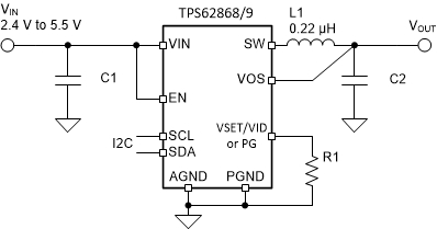
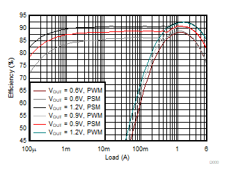
GUID-20200723-CA0I-D8JB-BFHD-V5SVQ9ZRQG7V-low.gifTypical Application
GUID-20200812-CA0I-LT6S-3NWZ-FXH2TPFJLJMV-low.gifEfficiency at VIN = 3.3 V